Microcontamination Control Solution by KAINOVA
| Brand | KAINOVA |
|---|---|
| Origin | Taiwan |
| Manufacturer Type | Authorized Distributor |
| Regional Classification | Asia-Pacific Sourced |
| Model | Kainova Tech – Microcontamination Control Solution |
| Pricing | Available Upon Request |
Overview
The KAINOVA Microcontamination Control Solution is an integrated suite of engineered subsystems designed to mitigate airborne molecular contamination (AMC), particle generation, and moisture ingress throughout semiconductor wafer handling and transfer processes. Operating on the principle of inert gas purging—primarily ultra-high-purity nitrogen (N₂) with dew point control below –70 °C and particulate filtration to ISO Class 1 (≤1 particle ≥0.1 µm per cubic foot)—this solution establishes and maintains controlled microenvironments at critical process interfaces: load ports, FOUP/SMIF openings, EFEMs, and automated material handling points. Unlike standalone filtration units, the KAINOVA system architecture implements dynamic pressure-balanced gas curtains, real-time flow monitoring, and closed-loop purge validation to ensure continuous compliance with SEMI F21-0719 (Guideline for Molecular Contamination Control in Semiconductor Manufacturing) and ISO 14644-8 Annex B (Chemical Contamination). It is deployed upstream of lithography, etch, and deposition tools where sub-10 nm node fabrication demands AMC levels below 0.1 ppb for basic amines, aldehydes, and sulfur compounds.
Key Features
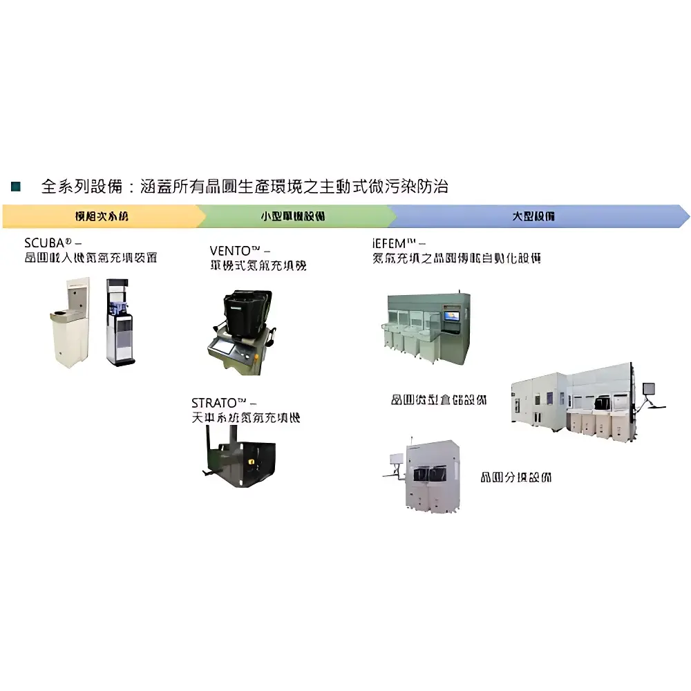
- Modular, scalable platform supporting integration into both legacy and next-generation 300 mm and 450 mm fab infrastructures
- SCUBA® Load Port Purge Module: Integrates with standard cluster tools; delivers laminar N₂ flow across FOUP interface with <100 ms response time to door-open events
- VENTO™ Standalone Purge Station: Benchtop unit with dual-chamber design for manual or semi-automated wafer cassette conditioning; includes built-in particle counter (0.05–5 µm) and dew point sensor (±0.5 °C accuracy)
- iEFEM™ Integrated EFEM Purge System: Fully automated, PLC-controlled purge sequence synchronized with robotic arm motion profiles; supports SECS/GEM communication and tool-to-tool handshaking
- STRATO™ Overhead Hoist Transport (OHT) Purge Interface: Enables in-transit contamination suppression during wafer transport between process modules; utilizes distributed nozzles with differential pressure feedback
- All subsystems comply with SEMI S2/S8 safety standards and feature redundant gas shut-off valves with SIL2-rated emergency response logic
Sample Compatibility & Compliance
The KAINOVA Microcontamination Control Solution is compatible with standard 300 mm FOUPs (SEMI E47.1), SMIF pods (SEMI E1.9), and advanced carrier formats including front-opening unified pods with RFID-enabled lids. It supports wafer thicknesses from 50 µm (ultra-thin Si) to 775 µm (power device substrates) and accommodates edge-exposed and bevel-clean configurations. All purge modules are validated per SEMI F22-0303 (Test Method for Evaluating Airborne Molecular Contaminant Removal Efficiency) and certified to ISO 9001:2015 and ISO 14001:2015. Documentation packages include IQ/OQ protocols traceable to NIST-calibrated reference instruments, supporting FDA 21 CFR Part 11-compliant audit trails when paired with optional KAINOVA LogVault™ software.
Software & Data Management
KAINOVA ControlSuite™ v4.2 provides centralized configuration, real-time diagnostics, and historical purge performance analytics across heterogeneous module deployments. The software features role-based access control (RBAC), encrypted data logging (AES-256), and native export to CSV, OPC UA, and MES-compatible XML schemas. Critical parameters—including purge flow rate (L/min), inlet/outlet dew point (°C), differential pressure (Pa), and particle counts per size bin—are timestamped with UTC synchronization and stored for ≥18 months. Audit logs record all operator actions, parameter changes, and alarm acknowledgments, fulfilling GLP/GMP requirements for traceability and root-cause analysis. Optional integration with factory-wide APC systems enables predictive maintenance alerts based on gas consumption trends and filter delta-P degradation modeling.
Applications
- Front-end-of-line (FEOL) lithography cell entry conditioning prior to stepper exposure
- Post-etch and post-CMP wafer stabilization to prevent watermark formation and metal ion adsorption
- High-k/metal gate stack processing where amine-induced threshold voltage shift must be suppressed
- Advanced packaging environments (e.g., fan-out wafer-level packaging) requiring low-halogen purge integrity
- Research cleanrooms conducting EUV mask handling and metrology where hydrocarbon outgassing compromises imaging fidelity
- Compound semiconductor fabs (GaN, SiC) sensitive to chlorine residue and moisture-induced surface oxidation
FAQ
Does the system support helium or argon as alternative purge gases?
Yes—gas manifold architecture is configurable for N₂, He, Ar, or forming gas (N₂/H₂); custom calibration and safety interlocks are required for non-nitrogen variants.
Can purge parameters be adjusted remotely via fab network?
Yes—ControlSuite™ supports secure TLS 1.3 remote access with two-factor authentication; parameter changes require supervisor-level approval and generate immutable audit entries.
Is validation support provided for ISO 14644-8 chemical classification?
KAINOVA supplies application-specific test plans aligned with ISO 14644-8 Annex B and ASTM D6369-20; third-party verification services are available through accredited partner labs.
What is the typical lead time for iEFEM™ integration into existing cluster tools?
Standard integration cycle is 8–12 weeks, including mechanical interface engineering, SECS/GEM protocol mapping, and FAT/SAT execution.
Are spare parts and consumables (e.g., filters, sensors) stocked regionally?
Yes—KAINOVA maintains regional spares hubs in Singapore, Tokyo, and Dresden with 48-hour air freight commitment for critical items.


