MVSystems HWCVD MVS Hot-Wire Chemical Vapor Deposition System
| Brand | MVSystems |
|---|---|
| Origin | USA |
| Manufacturer Type | Authorized Distributor |
| Origin Category | Imported |
| Model | MVS |
| Pricing | Available Upon Request |
Overview
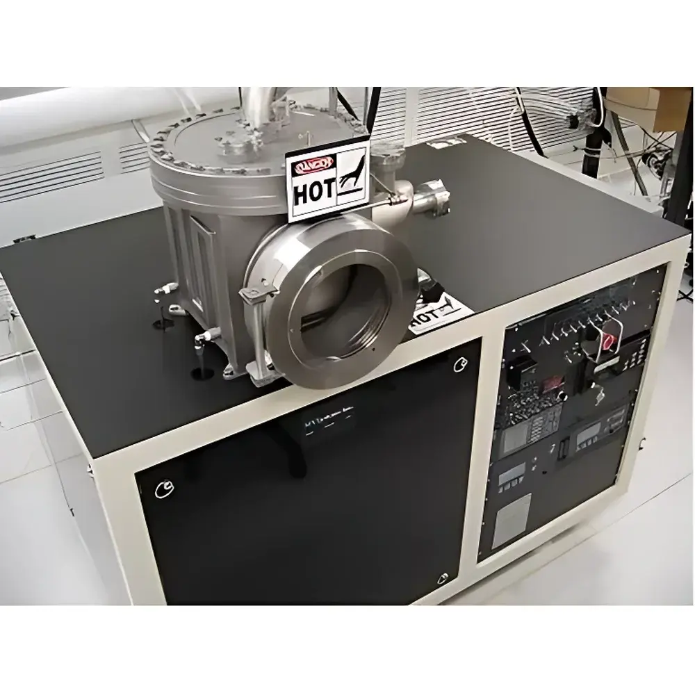
The MVSystems HWCVD MVS is a precision-engineered hot-wire chemical vapor deposition system designed for controlled, low-temperature synthesis of high-quality semiconductor thin films. Unlike plasma-enhanced CVD (PECVD), this system relies on catalytic thermal decomposition of precursor gases—such as silane (SiH₄), ammonia (NH₃), and phosphine (PH₃)—via resistively heated tungsten or tantalum filaments operating at temperatures between 1600 °C and 2200 °C. This thermally driven process enables highly uniform film growth with minimal ion bombardment damage, making it especially suitable for delicate substrates and metastable material phases including hydrogenated amorphous silicon (a-Si:H), nanocrystalline silicon (nc-Si:H), silicon nitride (SiNx), silicon oxide (SiOx), and transparent conductive oxides (TCOs). The MVS platform supports both single-chamber R&D configurations and modular integration into cluster-tool architectures—either star-type or linear layouts—ensuring scalability from laboratory prototyping to pilot-line manufacturing.
Key Features
- Modular chamber architecture compatible with standalone operation or integration into multi-process cluster tools (PECVD, PVD, sputtering)
- High-purity tungsten/tantalum filament array with independent temperature control and real-time thermal monitoring
- Computer-controlled gas delivery system with mass flow controllers (MFCs) for SiH₄, NH₃, H₂, PH₃, B₂H₆, and other reactive precursors
- Integrated vacuum system with base pressure <5×10⁻⁷ Torr and process pressure range of 0.1–10 Torr
- Substrate heating stage with programmable temperature control up to 400 °C, equipped with thermocouple feedback and uniformity calibration
- Full remote operation via Ethernet-connected industrial PC running custom LabVIEW-based control software
- Compliance-ready design supporting audit trails, user access levels, and electronic signature functionality aligned with GLP/GMP practices
Sample Compatibility & Compliance
The HWCVD MVS accommodates substrates up to 300 mm in diameter (or rectangular formats up to 30 cm × 40 cm) including glass, silicon wafers, stainless steel foils, and flexible polymer substrates. It is routinely employed in the fabrication of photovoltaic absorber layers, passivation stacks, gate dielectrics, and TCO electrodes—materials that must meet stringent industry specifications such as ASTM E2848 (PV performance testing), ISO 15667 (thin-film metrology), and IEC 61646 (thin-film PV module qualification). All gas-handling components conform to SEMI F57 standards for hazardous gas safety, and the system includes redundant leak detection, automatic shutoff valves, and exhaust scrubbing interfaces for silane and other pyrophoric gases.
Software & Data Management
The MVS operates under MVSystems’ proprietary deposition management suite, which provides synchronized logging of filament current/voltage, substrate temperature, chamber pressure, gas flows, and deposition time with millisecond resolution. Raw data are stored in HDF5 format with embedded metadata (user ID, timestamp, recipe ID, calibration references), enabling traceability per FDA 21 CFR Part 11 requirements. Export options include CSV, MATLAB .mat, and ASCII for post-processing in Origin, Python (NumPy/Pandas), or JMP. Optional add-ons include automated recipe validation, inter-chamber consistency reporting, and integration with enterprise MES platforms via OPC UA.
Applications
- Growth of intrinsic and doped a-Si:H and nc-Si:H for tandem solar cells and TFT backplanes
- Deposition of stoichiometric SiNx and SiOx for surface passivation and anti-reflection coatings
- Low-damage synthesis of TCOs (e.g., ITO, AZO) on temperature-sensitive substrates
- Fabrication of buffer layers in perovskite/silicon hybrid photovoltaics
- R&D of novel chalcogenide and oxide semiconductors requiring precise H-content control
- Process development for roll-to-roll and large-area photovoltaic manufacturing lines
FAQ
What substrates can be processed in the MVS system?
Standard configurations support rigid and flexible substrates up to 30 cm × 40 cm; custom stages accommodate wafer sizes up to 300 mm.
Is silane handling certified for Class 2B hazardous gas protocols?
Yes—the system integrates dual-stage pressure regulation, continuous infrared gas monitoring, and fail-safe purge sequences compliant with NFPA 55 and CGA G-13.
Can the MVS be upgraded to include in-situ diagnostics?
Absolutely—optional add-ons include real-time optical emission spectroscopy (OES), residual gas analysis (RGA), and laser interferometric thickness monitoring.
Does MVSystems provide application support for new material development?
Yes—customers gain access to MVSystems’ technical team for process optimization, film characterization guidance, and joint IP development under NDA.
Are service contracts and remote diagnostics available internationally?
Global support includes annual preventive maintenance, firmware updates, and secure remote troubleshooting via encrypted VNC sessions with audit-log generation.


