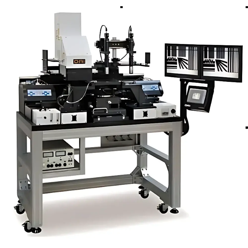
OAI MODEL 800MBA Dual-Side Alignment Mask Aligner
| Brand | OAI |
|---|---|
| Origin | USA |
| Model | MODEL 800MBA |
| Exposure Modes | Proximity, Soft Contact, Hard Contact, Vacuum Contact |
| Maximum Mask Size | 9" × 9" (228.6 mm × 228.6 mm) |
| Maximum Wafer Size | 200 mm (8-inch) |
| Light Source Type | High-Uniformity Broadband UV Lamp System |
| Alignment Accuracy | ≤ ±0.5 µm (typical, with optional auto-alignment upgrade) |
| Baseplate Thermal Stability | < ±0.1 °C over 4 hours |
| Compliance | ASTM F39–22 (Photolithography Equipment), ISO 14644–1 Class 5 Cleanroom Compatible |
Overview
The OAI MODEL 800MBA Dual-Side Alignment Mask Aligner is a precision photolithography instrument engineered for high-fidelity, repeatable double-sided patterning of semiconductor wafers up to 200 mm in diameter. Operating on the principle of contact and proximity photolithography, the system utilizes broadband ultraviolet (UV) illumination—typically spanning 320–450 nm—with exceptional spatial uniformity (< ±2% across full field) and minimal divergence. Unlike projection-based steppers or scanners, the 800MBA employs mask-to-wafer alignment via high-resolution optical microscopes (10×–50× magnification, motorized X/Y/Z/θ adjustment) and mechanical registration systems, enabling sub-micron overlay accuracy under controlled environmental conditions. Designed for R&D laboratories, pilot lines, and specialty device fabrication (e.g., MEMS, power devices, compound semiconductors), it supports process flexibility without requiring cleanroom-grade infrastructure—though optimal performance is achieved in ISO Class 5 or better environments.
Key Features
- Dual-side alignment capability with independent top- and bottom-side microscopes, each equipped with coaxial illumination and motorized focus/translation stages
- Four exposure modes: proximity (gap-controlled, 10–50 µm), soft contact (light membrane-assisted), hard contact (direct quartz-glass contact), and vacuum contact (≤10⁻² Torr chamber pressure for zero-gap registration)
- Integrated high-stability UV source (OAI proprietary arc lamp or LED-based option) with real-time radiometric monitoring and closed-loop intensity regulation
- Programmable exposure timer (0.1 s–9999.9 s resolution) synchronized with shutter actuation and vacuum sequencing
- Thermally isolated granite baseplate with active temperature stabilization (±0.1 °C drift over 4 h), minimizing thermal drift during multi-step alignment
- Manual and semi-automated operation modes; compatible with third-party vision software APIs for integration into automated metrology workflows
Sample Compatibility & Compliance
The MODEL 800MBA accommodates standard semiconductor substrates including silicon, SiC, GaAs, quartz, and glass wafers from 100 mm to 200 mm diameter, with thicknesses ranging from 200 µm to 1.5 mm. It accepts masks up to 9″ × 9″ (228.6 mm × 228.6 mm) in fused silica or low-thermal-expansion glass. The system meets ASTM F39–22 requirements for mask aligner performance verification—including intensity uniformity mapping, critical dimension repeatability, and alignment reproducibility testing. It operates within ISO 14644–1 Class 5 cleanroom specifications when installed with appropriate laminar airflow enclosures. Optional upgrades support GLP/GMP-compliant operation, including audit-trail-enabled software logging per FDA 21 CFR Part 11 requirements.
Software & Data Management
Control is managed via OAI’s Windows-based AlignPro™ software suite, which provides intuitive GUI-driven workflow management, exposure recipe storage (with user-defined naming, versioning, and metadata tagging), and real-time intensity calibration logs. All alignment parameters—including microscope coordinates, gap settings, exposure duration, and lamp energy dose—are timestamped and exportable in CSV or XML format. The software supports password-protected operator roles (e.g., Technician, Engineer, Admin), electronic signature capture for SOP execution, and optional integration with MES platforms via OPC UA or RESTful API endpoints. Raw image data from alignment cameras may be archived locally or pushed to network-attached storage with configurable retention policies.
Applications
- Development and prototyping of double-sided MEMS structures (e.g., accelerometers, pressure sensors, RF filters)
- Fabrication of high-voltage power devices requiring through-wafer metallization and backside alignment
- Research in flexible electronics using thin-film transistor (TFT) patterning on polyimide or glass substrates
- Production of optoelectronic components such as VCSEL arrays and photodetector hybrids where front/back interconnect alignment is critical
- University and government lab use in nanotechnology, quantum device fabrication, and radiation-hardened IC development
FAQ
What wafer thicknesses can the MODEL 800MBA accommodate?
Standard chuck configuration supports wafers from 200 µm to 1.5 mm thick; custom chucks are available for ultra-thin (<100 µm) or warped substrates.
Is vacuum contact mode compatible with fragile or porous substrates?
Yes—vacuum level and ramp rate are fully programmable to prevent substrate deformation or outgassing damage during contact establishment.
Can the system be upgraded to support automated mask loading?
OAI offers the AutoLoad™ module as a factory-installed retrofit, enabling cassette-to-chuck transfer with SECS/GEM protocol support.
Does the aligner include radiometric calibration traceability?
Each unit ships with NIST-traceable UV irradiance calibration certificate; annual recalibration services are available through OAI’s ISO/IEC 17025-accredited service centers.
What maintenance intervals are recommended for the UV lamp and optics?
Lamp lifetime is rated at ≥1,000 hours at nominal output; quartz optics cleaning and alignment verification are recommended every 200 hours of operation or per quarterly preventive maintenance schedule.


