Photonic Lattice WPA-100 Series Photoelastic Stress Analyzer
| Brand | Photonic Lattice |
|---|---|
| Origin | Japan |
| Model | WPA-100, WPA-100-L, WPA-100-S |
| Measurement Range | 0–4000 nm |
| Repeatability | <1.0 nm |
| Pixel Resolution | 384 × 288 |
| Wavelength Options | 523 nm, 543 nm, 575 nm |
| Max Field of View (WPA-100) | 100 × 136 mm |
| Max Field of View (WPA-100-L) | 250 × 340 mm |
| Max Field of View (WPA-100-S) | 11.6 × 15.8 mm |
| Dimensions (WPA-100) | 310 × 466 × 605.5 mm |
| Dimensions (WPA-100-L) | 450 × 593 × 915.5 mm |
| Dimensions (WPA-100-S) | 200 × 275 × 309.5 mm |
| Weight (WPA-100) | 20 kg |
| Weight (WPA-100-L) | 26 kg |
| Weight (WPA-100-S) | 4 kg (unit) + 9 kg (power supply) |
| Data Interface | GigE (camera), RS232C (motor control) |
| Power Supply | AC 100–240 V, 50/60 Hz |
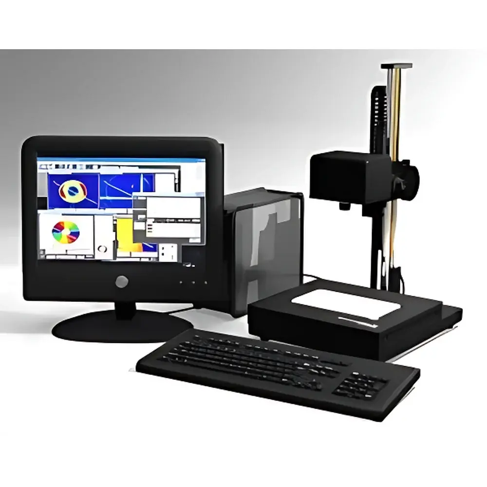
| Software | WPA-View |
Overview
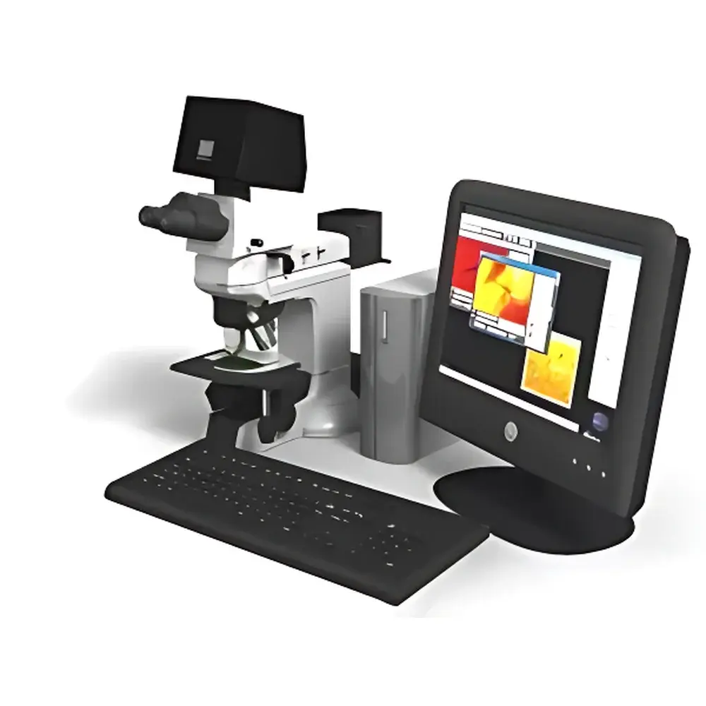
The Photonic Lattice WPA-100 Series Photoelastic Stress Analyzer is a high-precision, quantitative polarimetric imaging system engineered for the non-contact, full-field measurement of birefringence-induced phase retardation (δ) and its spatial distribution—including magnitude, orientation, and sign—across transparent and semi-transparent optical materials. Based on calibrated photoelasticity principles and digital polarization modulation, the WPA-100 employs a rotating waveplate configuration combined with a monochrome CMOS camera and tunable narrowband LED illumination (523 nm, 543 nm, or 575 nm) to extract retardation values via Fourier analysis of intensity modulations across four or more polarization states. This method ensures traceable, linear response over a dynamic range of 0–4000 nm with sub-nanometer repeatability (<1.0 nm), enabling detection of residual stress as low as ~0.01 MPa in fused silica or ~0.1 MPa in polycarbonate—critical for process validation in precision optics manufacturing.
Key Features
- Quantitative full-field retardation mapping at native resolution (384 × 288 pixels) with pixel-level orientation vector output
- Multi-wavelength capability (523 nm, 543 nm, 575 nm) supports dispersion-aware analysis and material-specific calibration
- Three modular configurations: WPA-100 (standard field), WPA-100-L (extended 250 × 340 mm FOV), and WPA-100-S (dedicated micro-optics mode for ≤10 mm lenses with automated circular ROI selection)
- Gigabit Ethernet interface for real-time image streaming and synchronized motor control via RS232C
- Robust mechanical architecture with vibration-damped optical baseplate and temperature-stabilized LED sources for long-term measurement stability
- Compliance-ready design: software timestamps, user access logs, and audit trail export in WPA-View support GLP/GMP-aligned workflows
Sample Compatibility & Compliance
The WPA-100 series accommodates planar and mildly curved transparent substrates up to 50 mm thick, including optical glass (e.g., BK7, SF11), crystalline wafers (SiO₂, CaF₂), polymer films (PC, PET, COP), injection-molded resin lenses, and semiconductor-grade quartz substrates. Sample mounting is gravity-based or vacuum-assisted; no clamping-induced artifact generation. The system conforms to ISO 11477 (plastics — determination of birefringence), ASTM D4093 (standard test method for birefringence of transparent plastics), and JIS R3203 (optical glass stress evaluation). All firmware and WPA-View software are developed under IEC 62304-compliant processes; raw data files include embedded metadata (wavelength, exposure, polarization sequence, calibration ID) to satisfy FDA 21 CFR Part 11 requirements for electronic records and signatures when deployed in regulated QC environments.
Software & Data Management
WPA-View is a Windows-based application providing real-time acquisition, multi-layer visualization (retardation magnitude, fast-axis orientation, isoclinic/isochromatic overlays), batch processing, and export to CSV, TIFF, or HDF5 formats. It includes built-in tools for region-of-interest (ROI) statistics, line-profile extraction, pass/fail thresholding with configurable tolerance bands, and automated defect flagging (e.g., “phase discontinuity” or “exceeds 3000 nm” alerts). Calibration routines follow NIST-traceable procedures using certified quarter-wave and half-wave standards. Audit logs record operator ID, timestamp, parameter changes, and export actions—exportable as encrypted PDF or XML for internal QA review or regulatory submission.
Applications
- Residual stress mapping in precision molded ophthalmic lenses to validate annealing cycles and prevent post-molding distortion
- In-line quality screening of display cover glass (Gorilla Glass®, aluminosilicate) for edge compression anomalies prior to lamination
- Process development support for wafer-level optics fabrication, including stress evaluation of anti-reflective coatings and bonding interfaces
- Failure analysis of polymer optical components subjected to thermal cycling or UV aging
- R&D characterization of photonic crystal slabs and metasurface substrates where local birefringence indicates lattice deformation or strain gradients
FAQ
What is the minimum detectable retardation under standard operating conditions?
The system achieves a noise-equivalent retardation (NER) of ≤0.3 nm RMS at 543 nm with 100 ms exposure, limited primarily by photon shot noise and polarization crosstalk.
Can the WPA-100 quantify stress directionality in anisotropic crystals?
Yes—the fast-axis orientation map resolves azimuthal angle with ±0.5° accuracy across the full FOV, enabling separation of intrinsic crystal birefringence from applied mechanical stress contributions.
Is WPA-View compatible with automated factory data systems?
Yes—via TCP/IP API and configurable CSV/XML export hooks, WPA-View integrates with MES platforms (e.g., Siemens Opcenter, Rockwell FactoryTalk) for SPC charting and OEE tracking.
Does the system require periodic recalibration?
Annual verification using supplied NIST-traceable reference standards is recommended; daily zero-check routines are automated within WPA-View.
How is thermal drift mitigated during extended measurements?
LED sources operate in constant-current mode with active thermal regulation; optical path length is stabilized via low-expansion aluminum alloy housing and passive thermal mass design.


