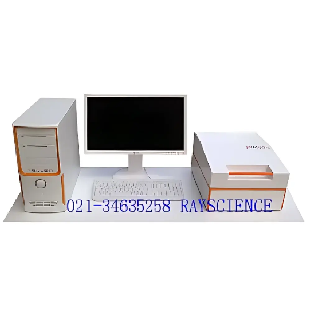
PVOTools 4PP-SCAN Four-Point Probe Sheet Resistance Mapping System
| Origin | Germany |
|---|---|
| Manufacturer Type | Authorized Distributor |
| Origin Category | Imported |
| Model | 4PP-SCAN |
| Price Range | USD 13,500 – 68,000 (FOB Hamburg) |
| Automation Level | Semi-Automatic |
| Probe Tip Material | Tungsten Carbide |
| Tip Radius | 0.25 mm |
| Maximum Test Current | 30 mA |
| Mapping Grid | 10 × 10 points |
| Typical Map Duration | 4 min |
| Vacuum Chuck | Tempered Glass with Integrated Vacuum Port |
| Dimensions (L×W×H) | 36 × 48 × 24 cm |
| Weight | 16 kg |
Overview
The PVOTools 4PP-SCAN is a semi-automated four-point probe (4PP) sheet resistance mapping system engineered for routine process control and inline quality assurance in semiconductor fabrication, thin-film R&D, and photovoltaic manufacturing environments. It operates on the classical van der Pauw / four-point collinear probe principle: two outer probes inject a known current while two inner probes measure the resulting voltage drop—enabling contactless, non-destructive quantification of surface resistivity (ρs, in Ω/□) without correction factors for homogeneous, isotropic, and sufficiently large samples. Unlike single-point handheld probes, the 4PP-SCAN integrates motorized X-Y stage positioning with programmable probe head actuation to generate spatially resolved resistivity maps—critical for identifying edge effects, coating non-uniformity, annealing gradients, or lithographic defects across wafers up to 150 mm (6-inch) diameter. Its modular architecture supports co-location with complementary metrology modules (e.g., TLM-SCAN++ for transfer length method characterization), enabling multi-parameter correlation within a single platform footprint.
Key Features
- Semi-automated mapping workflow: Fully programmable 10 × 10 grid acquisition with auto-triggering upon lid closure—eliminating manual start commands and reducing operator-induced variability.
- Interchangeable probe heads: Quick-swap tungsten carbide probe assemblies (tip radius 0.25 mm) recognized automatically by firmware; no recalibration required between head changes.
- Optimized vacuum chuck: Chemically resistant tempered glass platen with distributed vacuum ports ensures flat, particle-free sample immobilization—critical for repeatable tip-to-surface contact force and minimal wafer warpage.
- Integrated current–voltage linearity verification: On-the-fly I–V sweep functionality validates Ohmic contact behavior prior to sheet resistance calculation—flagging non-linearities caused by Schottky barriers or surface contamination.
- Robust mechanical design: All motion components housed within a rigid aluminum frame; vibration-damped base minimizes positional drift during extended map acquisitions.
Sample Compatibility & Compliance
The 4PP-SCAN accommodates rigid planar substrates including silicon wafers (up to 150 mm), glass, sapphire, and ceramic carriers with thicknesses from 200 µm to 2 mm. It complies with ASTM F84–22 (Standard Test Method for Resistivity of Silicon Wafers Using the Four-Point Probe Technique) and ISO 10777:2021 (Semiconductor devices — Electrical measurement of semiconductor materials). While not certified for GMP production environments, its audit-ready software logs (timestamped raw I/V data, probe ID, operator ID, environmental metadata) support GLP-aligned documentation requirements. The system meets CE marking directives (2014/30/EU EMC, 2014/35/EU LVD) and RoHS 2015/863 compliance.
Software & Data Management
PVOTools ControlSuite v4.x provides intuitive, scriptable operation via Windows-based GUI. Mapping results are rendered in real time with user-selectable colormaps (jet, viridis, grayscale), overlaid with contour lines, histogram distributions, and cross-sectional line scans. Each pixel retains full I/V trace data—enabling post-acquisition reanalysis of contact quality or temperature-corrected resistivity. Single-point remeasurement is executed with one mouse click on any map location. Export formats include CSV (tabular point data), PNG/JPEG (annotated visuals), and HDF5 (structured binary for MATLAB/Python integration). Audit trails comply with FDA 21 CFR Part 11 principles: electronic signatures, immutable log files, and role-based access control (admin/operator modes).
Applications
- Process monitoring of sputtered/evaporated metal layers (Al, Ti, Cu) and transparent conductive oxides (ITO, AZO) on display and solar cell substrates.
- Uniformity assessment of doped polysilicon gates and ion-implanted source/drain regions pre- and post-anneal.
- Quality gate for roll-to-roll coated flexible electronics—validating lateral conductivity consistency across web lengths.
- Rapid screening of photoresist development uniformity via post-bake sheet resistance shifts in patterned lift-off processes.
- Educational use in microfabrication labs: Demonstrating dopant diffusion profiles, junction depth estimation (via spreading resistance approximation), and Hall effect prerequisite characterization.
FAQ
What wafer sizes does the 4PP-SCAN support?
Standard configuration handles 100 mm and 150 mm wafers; optional adapters accommodate 76 mm and 200 mm substrates with modified chuck geometry.
Can the system measure resistivity below 1 mΩ/□?
No—the 4PP-SCAN is optimized for the 10 mΩ/□ to 10 MΩ/□ range. Ultra-low-resistance films require specialized low-noise current sources and Kelvin sensing not integrated into this platform.
Is vacuum pump included?
Yes—a compact, oil-free diaphragm vacuum pump (ultimate pressure ≤ 50 mbar) is supplied with mounting bracket and noise-dampening enclosure.
How is probe alignment verified?
A built-in reference calibration wafer (certified Si with NIST-traceable ρs) is provided for daily performance verification; alignment drift is detectable via repeat-measurement standard deviation tracking in ControlSuite.
Does the software support automated pass/fail binning?
Yes—user-defined upper/lower ρs thresholds trigger color-coded pass (green)/fail (red) overlays and generate summary reports with yield statistics per map.


