Silicon-on-Sapphire (SOS) Wafers — Al₂O₃ + Si Thin-Film Substrates (100 mm, R-Plane Sapphire, Undoped Silicon)
| Brand | 合肥科晶 |
|---|---|
| Origin | USA |
| Manufacturer Type | Authorized Distributor |
| Origin Category | Imported |
| Model | Al₂O₃+Si Thin-Film (SOS) |
| Price | Upon Request |
| Si Orientation | <100> |
| Doping Type | Intrinsic (Undoped) |
| Si Thickness | 0.6 µm ± 0.06 µm |
| Si Resistivity | > 100 Ω·cm |
| Sapphire Substrate | R-plane Al₂O₃ with single flat |
| Sapphire Diameter | 100 mm |
| Sapphire Thickness | 0.53 mm |
| Surface Flatness | ≤ 10 µm |
| Parallelism | ≤ 20 µm |
| Surface Finish | Single-side polished |
| Projected C-axis Orientation | 45° ± 2° |
| Customization | Optional Si deposition on C-plane Al₂O₃ |
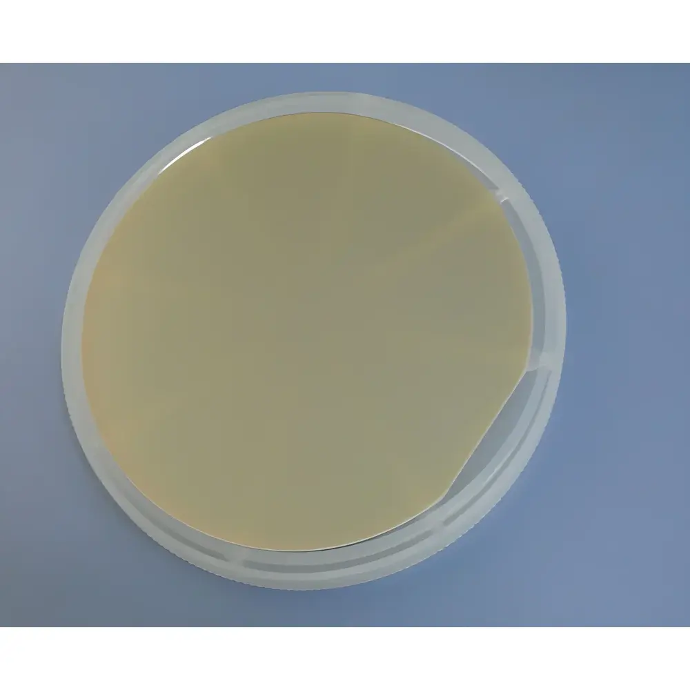
| Packaging | Vacuum-sealed in Class 100 cleanroom bags inside Class 1000 cleanroom environment or individual wafer cassettes |
Overview
Silicon-on-Sapphire (SOS) wafers represent a foundational substrate technology for high-performance radio-frequency (RF), radiation-hardened, and high-speed integrated circuits. This product is a precision-engineered heteroepitaxial structure consisting of a monocrystalline silicon thin film deposited on a single-crystal sapphire (Al₂O₃) substrate. The SOS architecture leverages the exceptional electrical insulation, thermal stability, and chemical inertness of sapphire—combined with the mature process compatibility of silicon—to enable low parasitic capacitance, high breakdown voltage, and superior isolation between active devices. Designed for use in RF SOI (Silicon-on-Insulator) applications, mixed-signal ASICs, MEMS integration platforms, and space-qualified electronics, these wafers are fabricated under strict semiconductor-grade cleanroom conditions to ensure atomic-level interface integrity and minimal defect density.
Key Features
- High-purity intrinsic silicon layer (0.6 µm ± 0.06 µm) with resistivity > 100 Ω·cm—optimized for low leakage and high carrier mobility.
- R-plane oriented sapphire substrate (Al₂O₃) with precisely controlled crystallographic alignment—ensures consistent epitaxial growth and reduced interfacial strain.
- Projected C-axis orientation of 45° ± 2° relative to the wafer surface—enables predictable lattice matching for subsequent Si epitaxy and device orientation control.
- Single-side polished finish on sapphire base—meets industry-standard surface roughness requirements for thin-film deposition and lithographic patterning.
- Tight dimensional tolerances: diameter 100 mm ± 0.1 mm, thickness 0.53 mm ± 0.01 mm, flatness ≤ 10 µm PV, parallelism ≤ 20 µm—critical for vacuum chucking, stepper alignment, and uniform thin-film processing.
- Class 100 cleanroom packaging: individually vacuum-sealed in laminar-flow-certified bags or stored in inert-gas purged wafer cassettes—minimizes particle contamination and oxide formation during storage and transport.
Sample Compatibility & Compliance
These SOS wafers are compatible with standard semiconductor fabrication tools—including MBE (Molecular Beam Epitaxy), CVD (Chemical Vapor Deposition), and PVD (Physical Vapor Deposition) systems—as well as photolithography, etching, and metrology platforms. The sapphire substrate exhibits excellent resistance to HF-based etchants and maintains structural integrity up to 1000 °C in inert atmospheres. The material complies with JEDEC standards for substrate dimensional stability and meets ISO 14644-1 Class 5 (ISO Class 5) cleanroom handling protocols. While not pre-certified for specific end-use regulatory frameworks, the intrinsic silicon layer and sapphire base support qualification under MIL-PRF-19500 (for discrete semiconductors), NASA EEE-INST-002 (space electronics), and ESA/SCC Basic Specification No. 22900 (radiation-tolerant substrates).
Software & Data Management
This is a passive substrate material—not an instrument—and therefore does not include embedded firmware, software interfaces, or data acquisition capabilities. However, full traceability documentation—including lot-specific crystallographic verification reports (XRD rocking curve FWHM, RHEED patterns), surface metrology data (AFM RMS roughness, optical interferometry maps), and cleanroom environmental logs—is provided upon request. All documentation conforms to GLP-compliant record retention practices and supports audit readiness for ISO 9001:2015 quality management systems. For customers requiring digital integration, metadata (e.g., wafer ID, orientation angle, thickness map coordinates) can be delivered in CSV or SEMI E142-compliant XML format for ingestion into MES (Manufacturing Execution Systems) or LIMS environments.
Applications
- RF front-end modules (FEMs) and power amplifiers in 5G/6G infrastructure where high Q-factor and low insertion loss are essential.
- Radiation-tolerant microcontrollers and FPGAs for satellite avionics and nuclear instrumentation.
- High-voltage analog switches and RF MEMS resonators requiring dielectric isolation beyond conventional SOI.
- Quantum device test platforms leveraging sapphire’s low dielectric loss tangent (tan δ ≈ 0.0001 at 10 GHz) and ultra-low microwave absorption.
- Research-grade substrates for heterostructure growth studies, including strained-Si, Ge-on-Si, and 2D material transfer (e.g., graphene, h-BN).
FAQ
What does “R-plane sapphire” mean, and why is it used for SOS?
R-plane sapphire refers to the (11̅02) crystallographic orientation of Al₂O₃. It provides optimal lattice matching for silicon growth with minimized dislocation density compared to C-plane or A-plane alternatives—making it the preferred choice for high-quality SOS epitaxy.
Can these wafers be used directly in CMOS fabrication lines?
Yes—they are compatible with standard 100 mm wafer handling equipment and meet front-end-of-line (FEOL) cleanliness specifications when unpacked in Class 100 environments. Thermal budget compatibility extends to standard gate oxidation and annealing steps.
Is the silicon layer grown or bonded?
The silicon film is epitaxially grown via high-temperature CVD or MBE on the sapphire substrate—not transferred or bonded—ensuring monolithic crystallinity and interface abruptness.
Do you offer custom Si thicknesses or doping profiles?
Yes—custom epitaxial layers (e.g., 0.3–2.0 µm Si, phosphorus-doped or boron-doped variants) are available under NDA with lead times of 8–12 weeks.
How is orientation verified prior to shipment?
Each wafer undergoes X-ray diffraction (XRD) theta-2theta scanning and pole figure analysis to confirm projected C-axis angle and mosaic spread—certification reports accompany every shipment.


