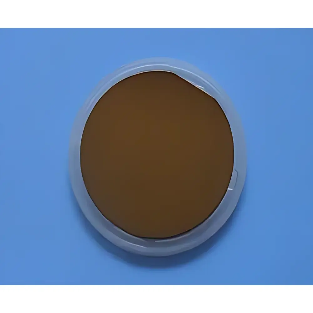
Si+Si3N4 Thin Film on P-type Silicon Wafer (PE-CVD, , 100 nm)
| Brand | Hefei Kejing |
|---|---|
| Origin | Anhui, China |
| Manufacturer Type | Authorized Distributor |
| Origin Category | Domestic |
| Model | Si+Si3N4 Thin Film |
| Pricing | Upon Request |
| Silicon Substrate | p-type Boron-doped, <100>±0.5°, Resistivity <0.02 Ω·cm, Single-side Polished, Thickness 525±25 µm, Diameter 101.6±0.5 mm |
| Silicon Nitride Layer | Low-stress PE-CVD deposited, 100 nm ±8%, Covers Front Polished Surface Only |
| Packaging | Class 1000 Cleanroom / Class 100 Clean Bag / Vacuum-Sealed / Individual Cassette or Slot-Style Rack |
Overview
The Si+Si₃N₄ thin film substrate is a precision-engineered silicon wafer platform designed for microelectromechanical systems (MEMS), nanofabrication, sensor development, and thin-film process qualification. It consists of a standard p-type boron-doped silicon wafer with a crystallographic orientation of ±0.5°, single-side polished surface, and a stoichiometric silicon nitride (Si₃N₄) layer deposited exclusively on the front polished side via low-stress plasma-enhanced chemical vapor deposition (PE-CVD). This architecture ensures mechanical stability, high dielectric strength (>7 MV/cm), and excellent thermal mismatch resistance—critical for reliable device release, etch masking, and passivation in reactive ion etching (RIE) and wet chemical processing environments. The substrate’s uniform thickness control (525±25 µm), tight resistivity specification (<0.02 Ω·cm), and ultra-low particulate packaging meet baseline requirements for cleanroom-compatible prototyping and pilot-line integration.
Key Features
- High-purity p-type silicon substrate with controlled boron doping and verified crystallographic alignment
- Low-stress PE-CVD silicon nitride film (100 nm ±8%) optimized for minimal intrinsic stress (<100 MPa compressive), reducing wafer bow and improving lithographic fidelity
- Front-side-only deposition preserves backside functionality for handling, alignment, or secondary processing (e.g., backside metallization or DRIE)
- Single-side polished finish (Ra <0.5 nm) enables high-resolution e-beam lithography and atomic layer deposition seeding
- Vacuum-sealed packaging in Class 100 clean bags within Class 1000 cleanroom environment minimizes organic contamination and particle adhesion
- Compatible with standard 4-inch wafer handling tools, aligners, and metrology platforms (e.g., ellipsometers, profilometers, SEM cross-sectioning)
Sample Compatibility & Compliance
This Si+Si₃N₄ substrate is compatible with common semiconductor fabrication protocols including buffered oxide etch (BOE), hot phosphoric acid stripping, and SF₆/O₂ RIE for selective Si₃N₄ patterning. Its electrical and structural specifications align with industry benchmarks defined in SEMI MF1530 (wafer flatness), SEMI MF1298 (resistivity measurement), and ISO 14644-1 Class 5 (equivalent to Federal Standard 209E Class 100) for packaging integrity. While not certified to ISO/IEC 17025, the material lot documentation includes traceable wafer ID, deposition run log, and post-deposition spectral reflectance verification—supporting GLP-compliant process documentation and internal QA audits.
Software & Data Management
No embedded firmware or proprietary software is associated with this passive substrate. However, it is fully interoperable with standard metrology data acquisition systems including Sentaurus Process, Lam Research SmartView, and Bruker Dektak step profiler software. Users may import wafer-level thickness maps, refractive index (n=2.0±0.03 at 633 nm), and extinction coefficient (k<0.001) into process simulation workflows. All physical lot records—including deposition chamber log files, ellipsometry calibration certificates, and cleanroom environmental monitoring summaries—are retained for 5 years per internal quality policy and available upon formal request for regulatory review.
Applications
- MEMS membrane and cantilever fabrication requiring high-tensile-strength dielectric membranes
- Capacitive pressure and inertial sensors where Si₃N₄ serves as both structural layer and hermetic barrier
- Maskless lithography test substrates for evaluating resist adhesion and etch selectivity
- Calibration reference wafers for FTIR, XPS, and spectroscopic ellipsometry system validation
- Seed layers for subsequent ALD Al₂O₃ or TiN deposition in gate-stack or MEMS encapsulation processes
- Platform for surface functionalization studies (e.g., silane monolayer grafting on Si₃N₄)
FAQ
Is the silicon nitride layer stoichiometric? What is its Si:N ratio?
Yes—the PE-CVD process is tuned to achieve near-stoichiometric Si₃N₄ (Si:N ≈ 3:4), confirmed by XPS analysis; minor nitrogen deficiency (<5% deviation) may occur at film edges due to chamber wall effects.
Can the backside be processed without damaging the front-side Si₃N₄?
Yes—backside lithography, metallization, or deep reactive ion etching (DRIE) is fully supported, provided front-side protection (e.g., photoresist or hard mask) is applied prior to aggressive backside chemistry.
What is the typical breakdown voltage of the Si₃N₄ film?
Measured DC breakdown field exceeds 7 MV/cm under point-probe testing at 100 nm thickness; actual device-level performance depends on electrode geometry and interface trap density.
Are custom thicknesses or doping profiles available?
Yes—Hefei Kejing offers OEM customization including Si₃N₄ thicknesses from 50–500 nm, alternate dopants (e.g., phosphorus-doped Si), and double-side polishing upon minimum order quantity agreement.
Does this substrate comply with RoHS or REACH directives?
Yes—all materials and processing chemicals used are RoHS-compliant; full substance declaration (SVHC screening) and REACH Annex XIV status documentation are provided with commercial orders.