
Scanning Probe Microscopes
Filter
Showing 61–90 of 110 results
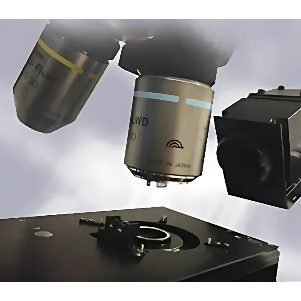
| Brand | Nanonics |
|---|---|
| Origin | Israel |
| Model | MultiView 2500 |
| Instrument Type | Hybrid SNOM/AFM System |
| Detection Noise (Positional) | 0.2 nm |
| Sample Size Capacity | 6 mm diameter |
| XYZ Scan Range per Stage | >80 µm |
| Dual-Stage Architecture | Probe Stage + Sample Stage |
| Feedback Mechanism | Tuning Fork (TF)-Based AFM |
| Optical Compatibility | Mid-IR to THz spectral range |
| Illumination/Collection Flexibility | Top-, Side-, and Bottom-Optical Access |
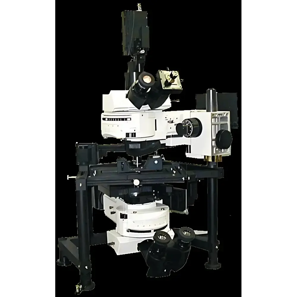
| Brand | Nanonics |
|---|---|
| Origin | Israel |
| Model | MultiView1000 |
| Instrument Type | Material-Focused AFM |
| Positional Noise | XY < 20 nm |
| Max Sample Diameter | < 100 mm |
| Max Sample Thickness | < 15 mm |
| Stage Travel Range | 85 µm × 85 µm |
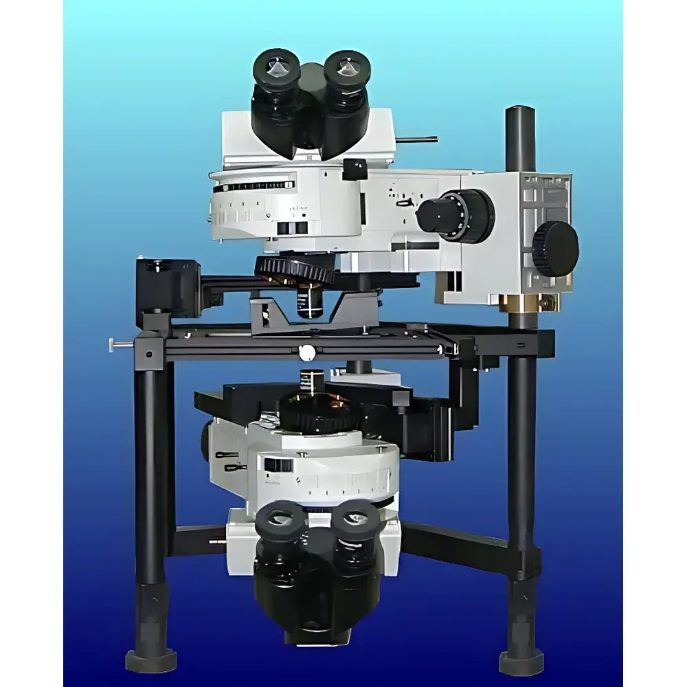
| Brand | Nanonics |
|---|---|
| Origin | Israel |
| Model | MultiView2000 |
| Instrument Type | Materials-Focused AFM/NSOM Hybrid System |
| Scan Mode | Tip Scanning |
| XY Resolution | <5 nm |
| Z Resolution | <1 nm |
| XY Scan Range | 70 µm (standard), optional 30 µm and 10 µm scanners |
| Z Scan Range | 70–120 µm |
| XY Step Size | <1 nm (70 µm scanner), <0.1 nm (10 µm scanner) |
| Scanner Thickness | 7 mm |
| Scanner Mass | 75 g |
| Max Sample Radius | 16 mm (customizable) |
| Probe Compatibility | Full commercial SPM probe interoperability including NSOM, conductive AFM, hollow probes, insulated nanowire sensors, dual-wire glass-insulated probes, low-k modulus probes, and deep-trench AFM probes |
| Operational Modes | NSOM reflection/transmission/collection/near-field fluorescence/PL |
| Controller | Nanonics Analog Controller with NT software (Windows 95/98/XP compatible) |
| Environmental Capabilities | Cryogenic operation down to 4 K (liquid helium), UHV compatibility, integrated gas/liquid delivery, in situ reaction chamber, co-located optical microscopy and micro-Raman coupling |
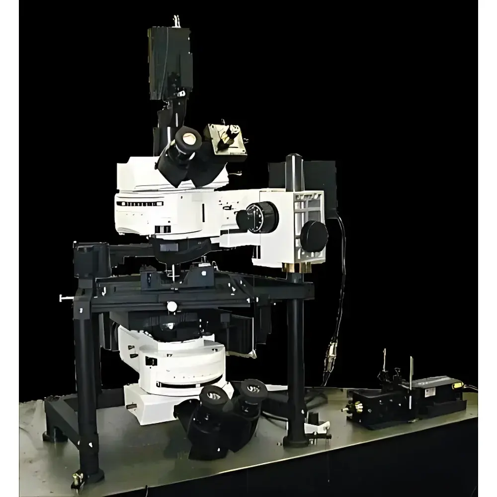
| Brand | Nanonics |
|---|---|
| Origin | Israel |
| Model | MultiView4000 |
| Instrument Type | Material-Focused AFM |
| Positioning Noise | XY < 20 nm |
| Sample Dimensions | Ø < 100 mm |
| Stage Travel Range | 170 µm × 170 µm |
| XY Resolution | < 5 nm |
| Z Resolution | < 1 nm |
| Scan Range (Combined Piezo + Sample Scanner) | up to 160 µm (XY) |
| Minimum Step Size | < 0.1 nm (10 µm scanner) |
| Scanner Thickness | 7 mm |
| Mass | 75 g |
| Probe Compatibility | Commercial SPM, NSOM, conductive, hollow, insulated glass nanowire, dual-wire, low-k AFM, deep-trench AFM probes |
| Operating Modes | NSOM reflection/transmission/collection/fluorescence/PL |
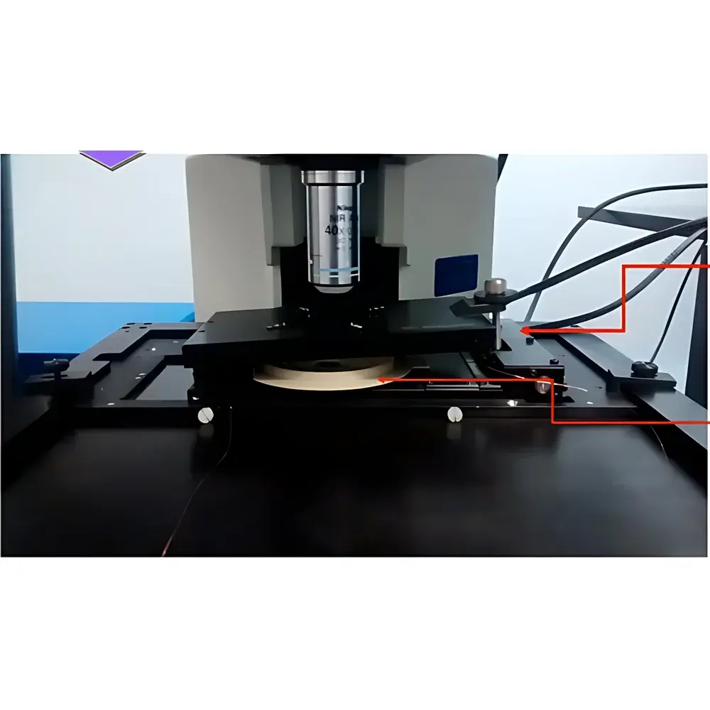
| Brand | Nanonics |
|---|---|
| Model | MV1000 / MV2000 / MV4000 |
| Instrument Type | AFM-Integrated Scanning Electrochemical Microscope |
| Z-Positioning Noise | 0.2 nm |
| Sample Diameter | < 6 mm |
| XYZ Scan Range | 80 µm × 80 µm × 80 µm |
| Probe | Hollow glass nanopipette with Pt nanowire electrode (50–100 nm tip diameter) |
| Electrochemical Control | Bipotentiostat (±10 V, ±0.25 A), current sensitivity: 10⁻¹²–0.1 A/V |
| Compatible Electrodes | Up to four side-mounted or back-contacted reference/counter electrodes (e.g., Ag/AgCl) |
| Liquid Cell Material | PEEK |
| Optical Access | Fully open top and bottom optical pathways |
| Environmental Options | Optional inert-gas chamber (N₂/Ar) |
| Software Compliance | Supports audit trail, user access control, and data integrity per FDA 21 CFR Part 11 requirements |
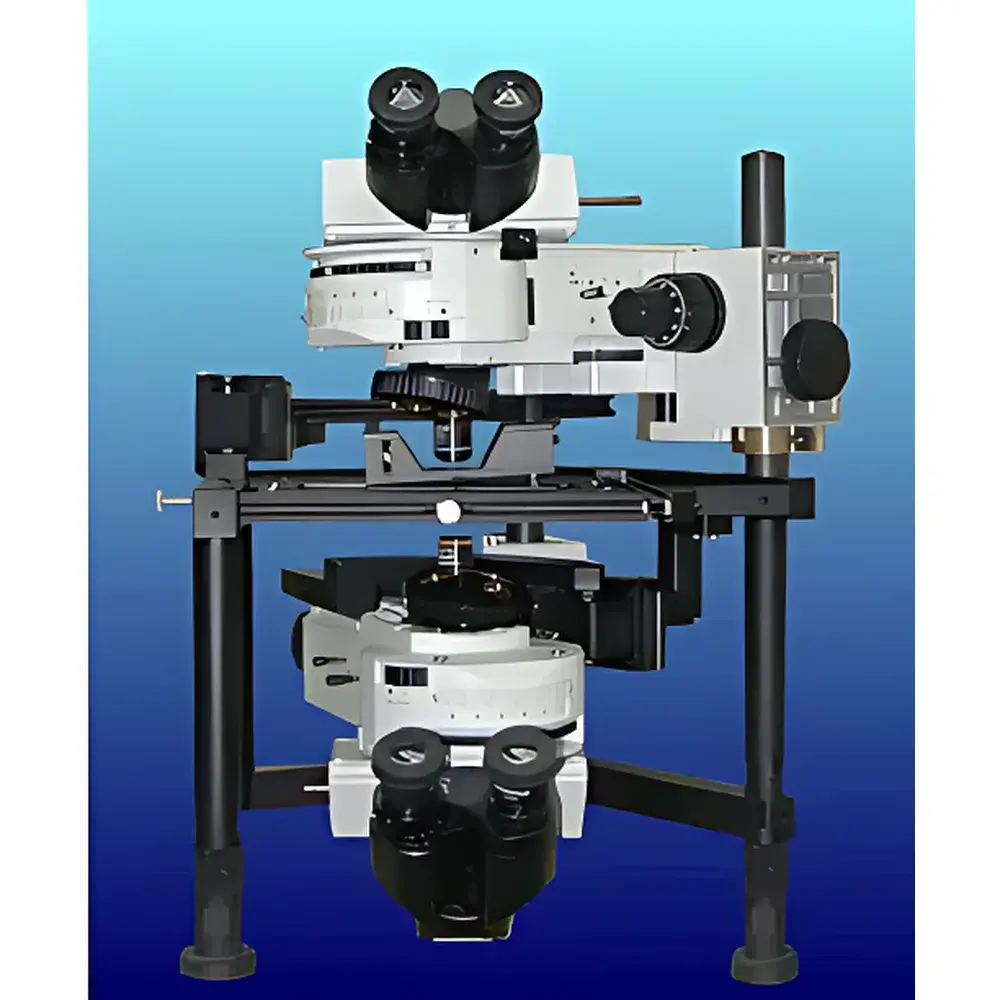
| Brand | Nanonics |
|---|---|
| Origin | Israel |
| Manufacturer Type | OEM Manufacturer |
| Origin Category | Imported |
| Model | MV2000 |
| Instrument Type | Materials-Focused Hybrid SPM Platform |
| Positional Detection Noise | 0.2 nm (RMS) |
| Maximum Sample Size | 6 mm (standard) |
| Sample Stage Scan Range | 80 µm × 80 µm × 80 µm (XYZ) |
| Z-Direction Resolution | < 0.05 nm (RMS) |
| XY Lateral Resolution (AFM) | < 0.15 nm |
| Near-Field Optical Resolution | ≤ 50 nm (aperture-limited) |
| Far-Field Optical Resolution | ~500 nm (non-confocal), ~200 nm (confocal) |
| Thermal Imaging Resolution | ≥ 100 nm |
| Electrical Resistance Mapping Resolution | ≥ 25 nm |
| Operating Temperature Range (Thermal Probes) | Up to 300 °C |
| Feedback Mechanism | Tuning Fork (standard), Laser Reflectance (optional) |
| Probe Compatibility | Glass fiber NSOM probes (patented bent-cantilever design), commercial Si/SiN AFM probes, custom multi-functional probes (optical/thermal/electrical/Raman-enhancing) |
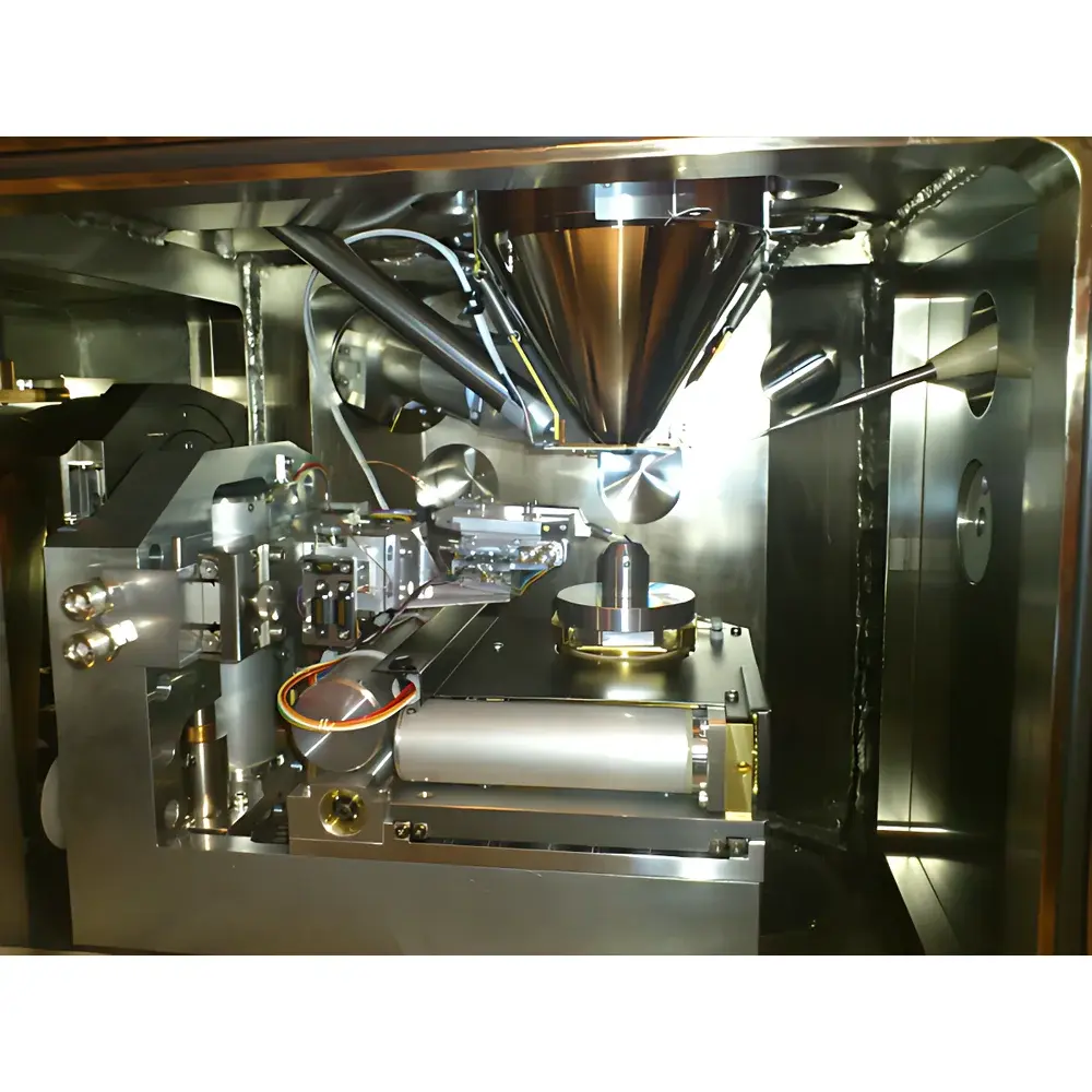
| Brand | Nanonics |
|---|---|
| Origin | Israel |
| Model | MV4000 |
| Instrument Type | Material-Focused Hybrid Correlative Microscope |
| Positional Detection Noise | 0.2 nm |
| Maximum Sample Diameter | <100 mm |
| Maximum Sample Thickness | <15 mm |
| Sample Stage Travel Range | 85 × 85 × 85 µm |
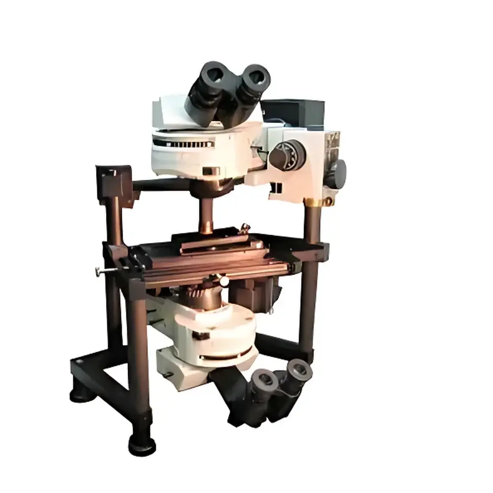
| Brand | Nanonics |
|---|---|
| Origin | Imported (Non-Chinese) |
| Model | NSOM |
| Instrument Type | Materials-Focused SPM Platform |
| Core Function | Scanning Near-Field Optical Microscopy (SNOM/NSOM) with Integrated AFM, Thermal, Electrical, and Raman Capabilities |
| Optical Resolution | ≤50 nm (near-field), 200 nm (confocal), diffraction-limited (far-field) |
| Scan Range | Up to 160 µm (XYZ, dual-probe configuration) |
| Z-Resolution | < 0.02 nm (XY), < 0.05 nm (Z, RMS) |
| Probe Types | Patented glass-fiber probes (metal-coated, hollow, TERS-optimized), compatible with commercial Si cantilevers |
| Feedback | Tuning fork (standard), laser reflection (optional) |
| Detector Compatibility | APD, PMT, InGaAs, CCD, spectrometers |
| Laser Range | Deep UV to NIR |
| Thermal Sensitivity | 0.01 °C |
| Electrical Resolution | < 25 nm (resistive imaging) |
| Max Z-Depth | 140 µm |
| Multi-Probe Support | Up to 4 independently controlled probes |
| Compliance | Designed for GLP/GMP-aligned workflows |
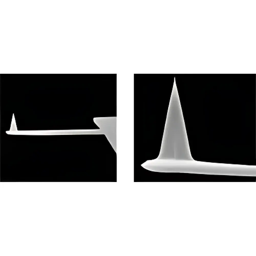
| Brand | Nanosensors (distributed by SHNTI) |
|---|---|
| Origin | Switzerland |
| Probe Type | Tapping Mode AFM Cantilevers |
| Substrate Material | Boron-Doped Silicon (5×10²⁰/cm³) |
| Substrate Dimensions | 1.6 mm × 3.6 mm × 0.4 mm |
| Reflective Coating | Au (3× reflectivity vs. uncoated) |
| Tip Radius | ≤10 nm (SEM-verified, S-series option available) |
| Tip Height | 10–15 µm |
| Cantilevers per Chip | 2 rectangular beams |
| Aspect Ratio | 3:1 |
| Half-Angle | ≤22° |
| Conductive Coating Options | TiN, W₂C, Pt, Au |
| Compatibility | Universal SPM platforms (Bruker, Keysight, Park Systems, NT-MDT, etc.) |
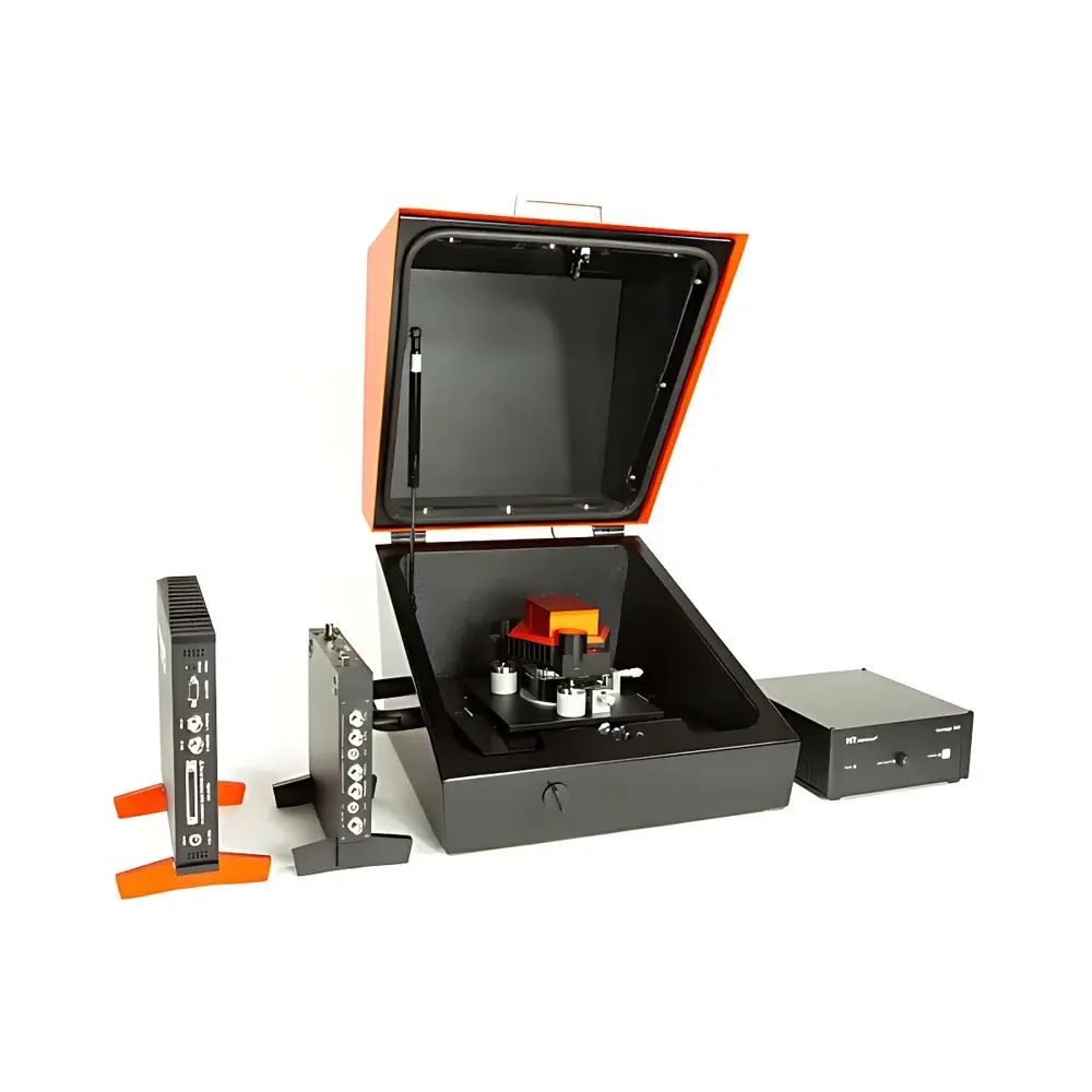
| Brand | Nanosurf |
|---|---|
| Origin | Switzerland |
| Model | FLEX-AFM |
| Instrument Type | Atomic Force Microscope |
| XY Positioning Noise | ≤ 0.15 nm (RMS, in air & liquid) |
| Sample Dimensions | Ø ≤ 100 mm, Thickness ≤ 5 mm |
| Sample Stage Travel Range | 300 mm × 300 mm |
| Scan Range | 100 µm × 100 µm × 10 µm (XY × Z) |
| XY Drive Resolution | 0.152 nm |
| Z Drive Resolution | 0.046 nm |
| Minimum Z Noise Floor | 0.15 nm (RMS, closed-loop) |
| Compatible Environments | Ambient air, liquid, controlled atmosphere (e.g., inert gas, low-oxygen), temperature-controlled stages |
| Controller | C3000 (24-bit, dual-channel lock-in amplifiers, digital feedback) |
| Optical Integration | Fully compatible with inverted optical microscopes |
| Modular Add-ons | ECS 204 electrochemical stage, ATS 204 automated translation stage, Isostage active vibration isolation, acoustic enclosure, glovebox integration kit |
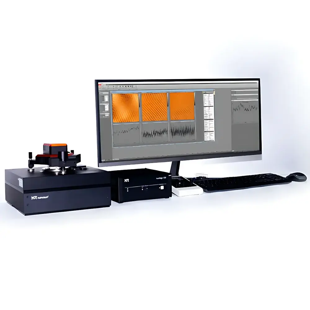
| Brand | Nanosurf |
|---|---|
| Origin | Switzerland |
| Model | FlexAFM |
| Instrument Type | Material-Focused AFM |
| Position Detection Noise | <35 pm |
| Maximum Sample Diameter | ≤120 mm |
| Control Electronics | C3000i (24-bit), upgradeable to CX (28-bit) |
| Software | Nanosurf Software Suite |
| Compliance | Designed for ISO/IEC 17025-aligned lab environments, supports GLP/GMP audit trails via optional software modules |
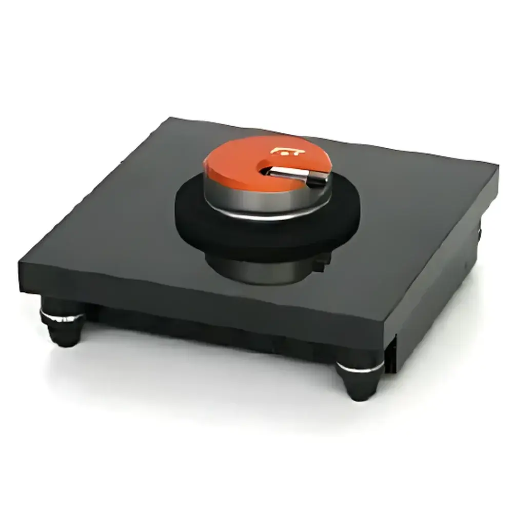
| Brand | Nanosurf |
|---|---|
| Origin | Switzerland |
| Model | Naio STM |
| Position Detection Noise | 0.15 nm |
| Sample Area | 500 nm × 500 nm |
| XY Scan Range | 500 nm × 500 nm |
| XY Resolution | 7.6 pm |
| Z Scan Range | 200 nm |
| Z Resolution | 3 pm |
| Maximum Tunneling Current | 100 nA |
| Sample Stage Diameter | 10 mm |
| Max Sample Thickness | 3 mm |
| Imaging Modes | Constant-Current & Constant-Height |
| Spectroscopy Modes | I–V, I–z |
| Max Image Pixels | 2048 × 2048 |
| Max Spectral Points | 32768 |
| XY Tilt Compensation | Hardware-based |
| Interface | USB 2.0 |
| Dimensions | 204 mm × 204 mm × 104 mm |
| Weight | 3.45 kg |
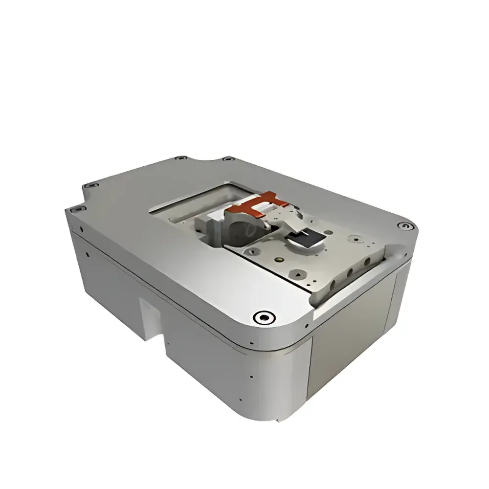
| Origin | Czech Republic |
|---|---|
| Manufacturer Type | Distributor |
| Origin Category | Imported |
| Model | LiteScope |
| Price Range | USD 65,000–130,000 |
| Instrument Type | Atomic Force Microscope |
| Positional Detection Noise | AFM-in-SEM Integration |
| Sample Dimensions | In-situ AFM-compatible |
| Stage Travel Range | 100 × 100 × 100 µm |
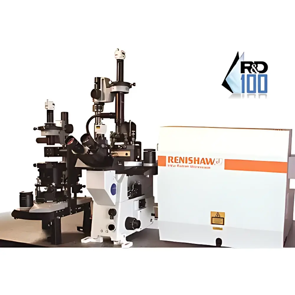
| Origin | Imported |
|---|---|
| Manufacturer Type | Authorized Distributor |
| Model | Ntegra Spectra |
| Pricing | Available Upon Request |
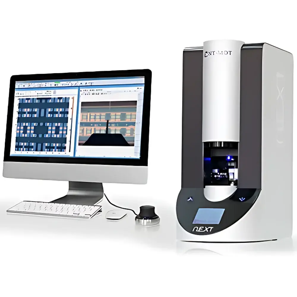
| Brand | NT-MDT |
|---|---|
| Origin | Russia |
| Model | Solver Next |
| Instrument Type | Atomic Force Microscope |
| Z-direction Position Detection Noise | 0.02 nm (low-current mode) |
| Maximum Sample Dimensions | Ø ≤ 20 mm, Height ≤ 10 mm |
| XY Sample Stage Travel Range | 5 mm × 5 mm |
| Scan Range (Closed-loop) | 100 µm × 100 µm × 10 µm |
| Z-noise (RMS, 10–1000 Hz) | ≤ 0.04 nm (closed-loop), 0.02 nm (low-current mode) |
| XY Nonlinearity | ≤ 0.1% (closed-loop) |
| Video Microscope Resolution | 2 µm |
| Temperature Control Range | Room Temperature to 150 °C |
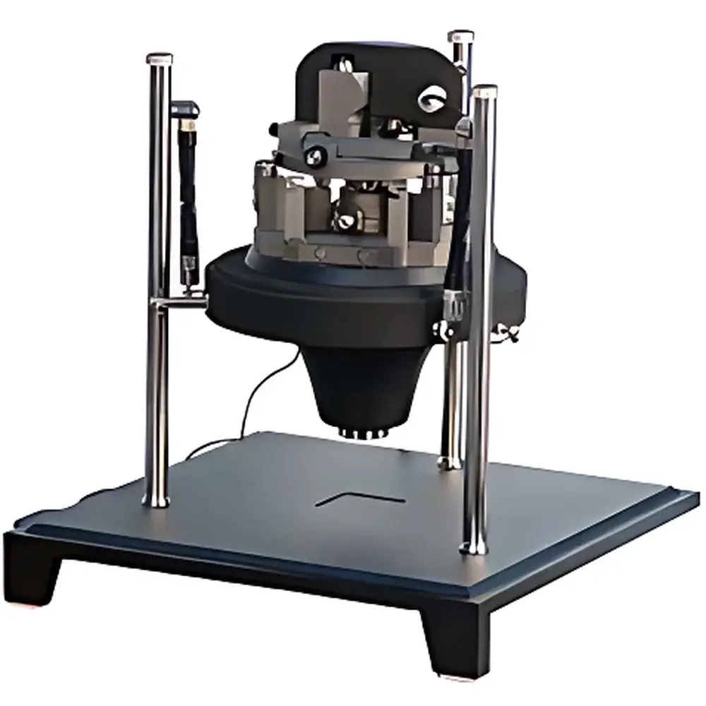
| Brand | NT-MDT |
|---|---|
| Origin | Imported |
| Manufacturer Type | Authorized Distributor |
| Model | Solver P47-Pro |
| Pricing | Available Upon Request |
| Measurement Modes | STM, AFM (Contact/Tapping/Non-contact), LFM, Phase Imaging, Force Modulation, Force Spectroscopy, Adhesion Mapping, MFM, EFM, Kelvin Probe, SSRM, Nanoindentation, Voltage/Force Nanolithography |
| Scanning Configurations | Sample Scanning, Tip Scanning, Dual-Scan Option |
| Max Sample Size (Sample Scan) | Ø40 mm × 10 mm |
| XY Sample Positioning Range | 5 × 5 µm |
| Positioning Accuracy | ±5 µm |
| Environmental Operation | Ambient Air, Controlled Atmosphere, Liquid Cell Compatible |
| Temperature Control | Room Temperature to 130 °C |
| Optical System | Custom-Configurable |
| SPM Techniques Supported | >40 Quantitative Modes |
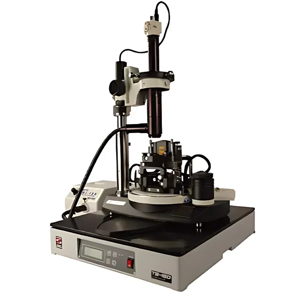
| Origin | Imported |
|---|---|
| Manufacturer Type | Authorized Distributor |
| Model | NTegra Platform Series (Prima, Aura, Therma, Maximus, Solaris, Vita, Tomo, Spectra) |
| Pricing | Available Upon Request |
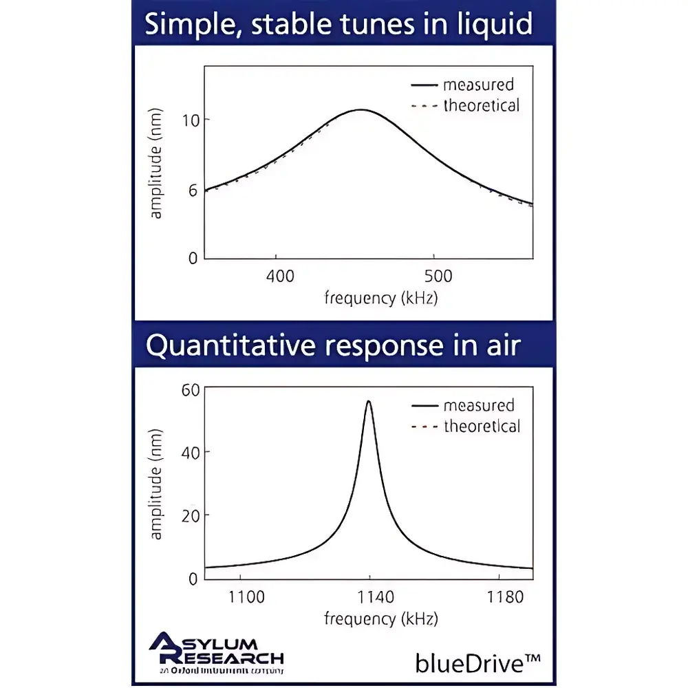
| Brand | Oxford Instruments |
|---|---|
| Origin | Germany |
| Manufacturer Type | Authorized Distributor |
| Origin Category | Imported |
| Model | blueDrive |
| Price Range | USD 13,500 – 68,000 |
| Instrument Type | AFM Accessory |
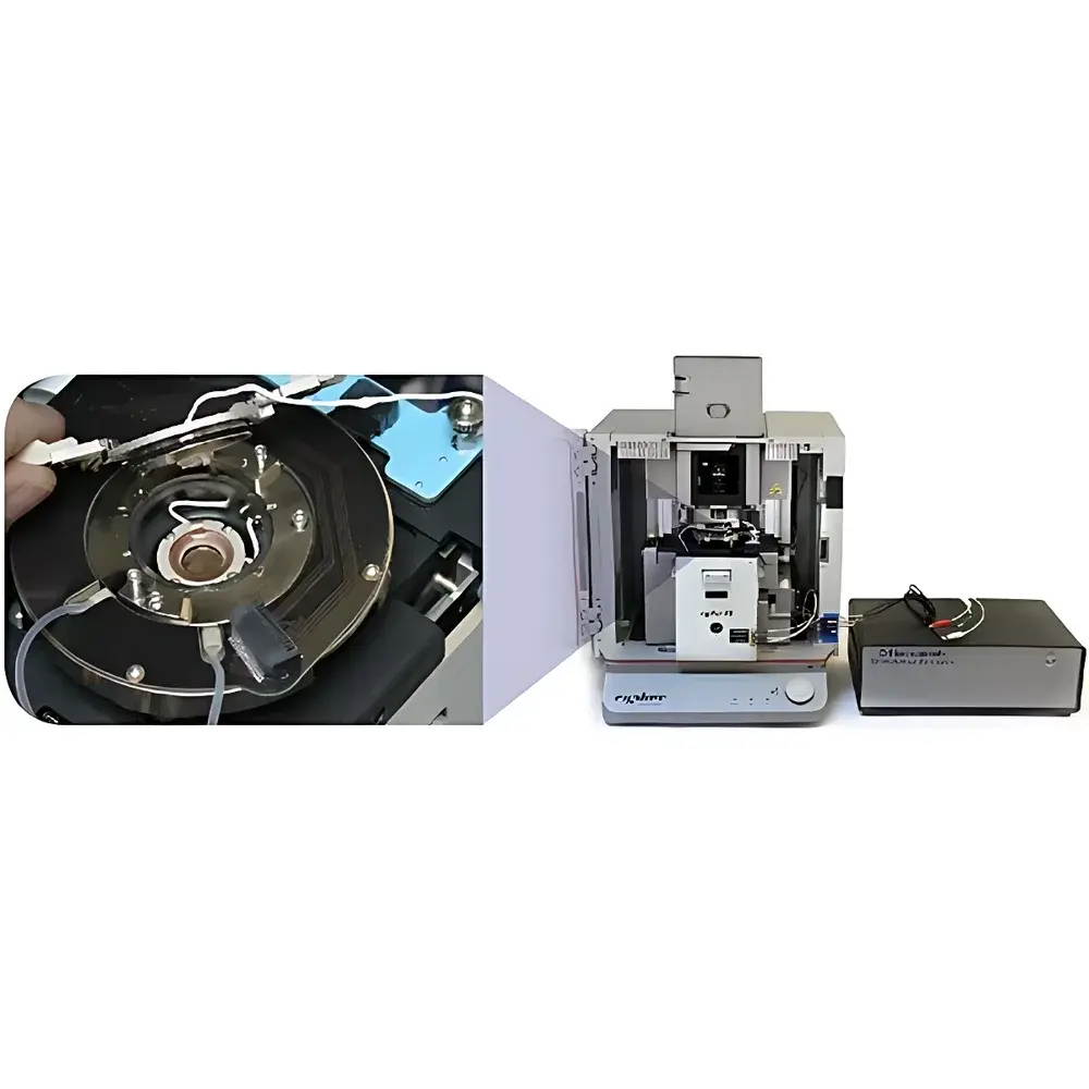
| Brand | Oxford Instruments |
|---|---|
| Origin | USA |
| Manufacturer Type | Authorized Distributor |
| Origin Category | Imported |
| Model | Cypher ES EC-AFM |
| Price Range | USD 340,000 – 410,000 (FOB) |
| Instrument Type | Atomic Force Microscope (AFM), Materials-Focused |
| Position Detection Noise | 625 Hz (RMS, bandwidth-corrected) |
| Sample Dimensions | Ø < 15 mm, Thickness < 5 mm |
| XY Stage Scan Range | 180 µm × 180 µm (optical field of view), with full 180 mm × 180 mm motorized sample positioning area |
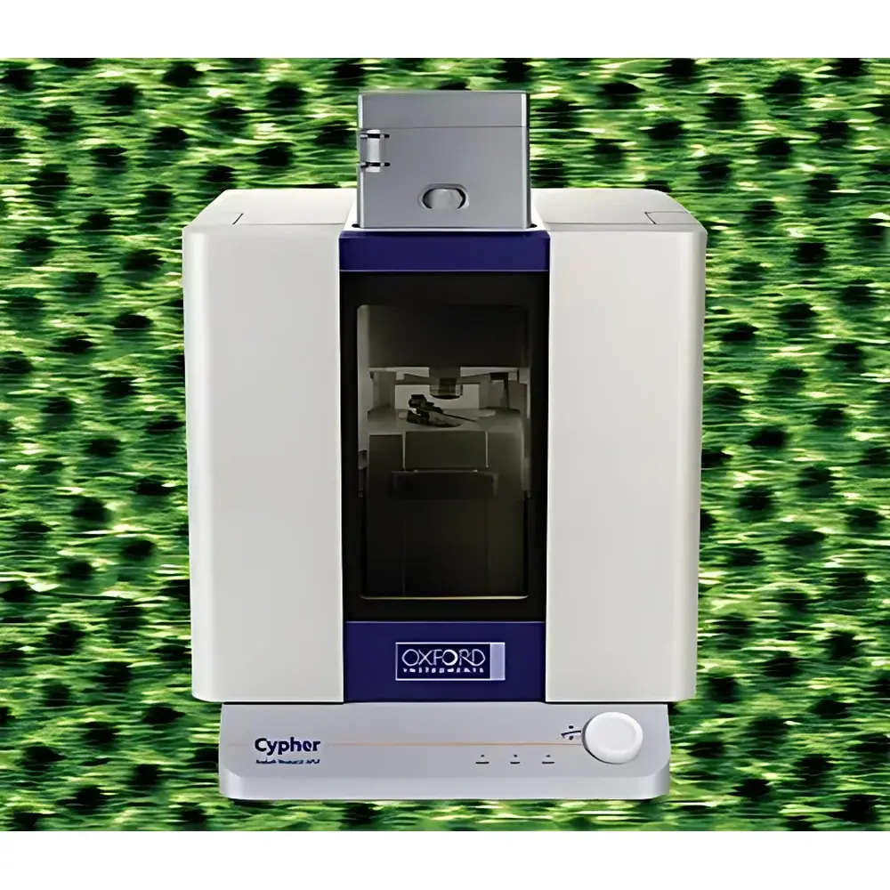
| Brand | Oxford Instruments |
|---|---|
| Origin | USA |
| Manufacturer Type | Authorized Distributor |
| Origin Category | Imported |
| Model | Cypher S |
| Instrument Type | Materials-Focused AFM |
| Closed-Loop Noise (X,Y) | <0.06 nm |
| Closed-Loop Noise (Z) | <0.05 nm |
| Height Noise | <0.015 nm |
| Sample Diameter | <15 mm (standard), <7 mm (high-stability configuration) |
| XY Stage Travel Range | 180 mm × 180 mm |
| Imaging Speed | Up to 10–100× faster than conventional AFMs |
| Probe Compatibility | Supports ultra-small probes (e.g., 3 × 9 µm optical spot size, optional) |
| Environmental Flexibility | Upgradeable to Cypher ES (environmental control) and Cypher VRS (video-rate scanning) |
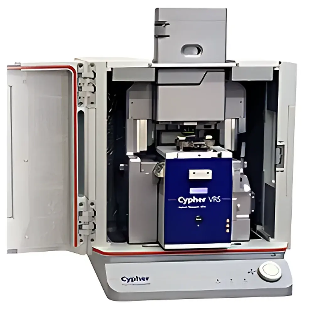
| Brand | Oxford Instruments |
|---|---|
| Origin | USA |
| Model | Cypher VRS |
| Instrument Type | Material-Focused Atomic Force Microscope |
| XY Positional Noise | <60 pm |
| Z Positional Noise | <50 pm |
| Maximum Sample Diameter | ≤15 mm |
| Maximum Sample Thickness | ≤7 mm |
| Sample Stage Travel Range | 180 mm × 180 mm |
| Scan Speed | Up to 625 lines/sec |
| Frame Rate | >10 fps at 512×512 pixel resolution |
| Excitation Method | blueDrive™ Photothermal Actuation |
| Compliance | ASTM E2539, ISO/IEC 17025-compatible operation, GLP/GMP-ready data integrity architecture |
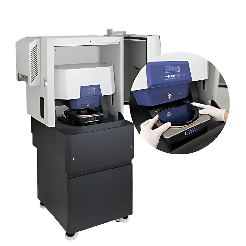
| Brand | Oxford Instruments |
|---|---|
| Origin | USA |
| Manufacturer Type | Authorized Distributor |
| Origin Category | Imported |
| Model | Jupiter XR |
| Price Range | USD 320,000 – 385,000 |
| Instrument Type | Atomic Force Microscope (AFM) |
| Application Class | Materials Science AFM |
| Position Detection Noise | 35 pm |
| Maximum Sample Diameter | 210 mm |
| XY Stage Travel Range | 200 mm × 200 mm |
| Scan Range | Up to 100 μm (full closed-loop) |
| Imaging Speed | 5–20× faster than conventional large-sample AFMs |
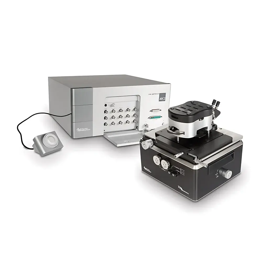
| Brand | Oxford Instruments |
|---|---|
| Origin | USA |
| Manufacturer Type | Authorized Distributor |
| Origin Category | Imported |
| Model | MFP-3D |
| Price Range | USD 135,000 – 205,000 (FOB) |
| Instrument Type | Atomic Force Microscope (AFM) |
| Application Class | Materials Science AFM |
| Z-Axis Positioning Noise | < 0.06 nm (RMS, in air) |
| X/Y Closed-Loop Scanning Noise | < 0.5 nm (RMS) |
| Sample Diameter | ≤ 80 mm |
| Sample Thickness | ≤ 25 mm |
| Visual Field of View | 200 mm × 200 mm (XY stage travel with optical alignment) |
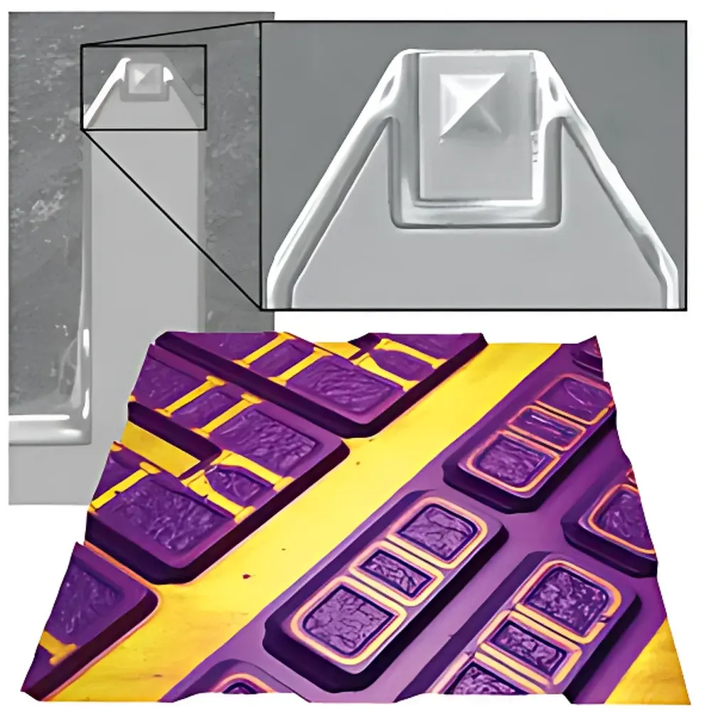
| Brand | Oxford Instruments |
|---|---|
| Origin | United Kingdom |
| Manufacturer Type | Authorized Distributor |
| Origin Category | Imported |
| Model | Scanning Microwave Impedance Microscopy (sMIM) |
| Instrument Type | Scanning Probe Microscope |
| Application Domain | Nanoscale Electrical Characterization |
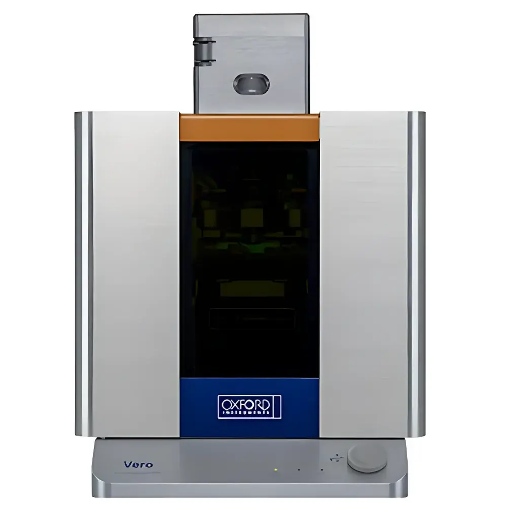
| Brand | Oxford Instruments |
|---|---|
| Origin | USA |
| Manufacturer Type | Authorized Distributor |
| Origin Category | Imported |
| Model | Vero |
| Price | Upon Request |
| Instrument Type | Atomic Force Microscope (AFM) |
| Application Class | Materials Science AFM |
| Position Detection Noise | X&Y Sensor Noise < 60 pm, Z Sensor Noise < 50 pm |
| Sample Dimensions | Up to 15 mm in diameter, 7 mm in thickness |
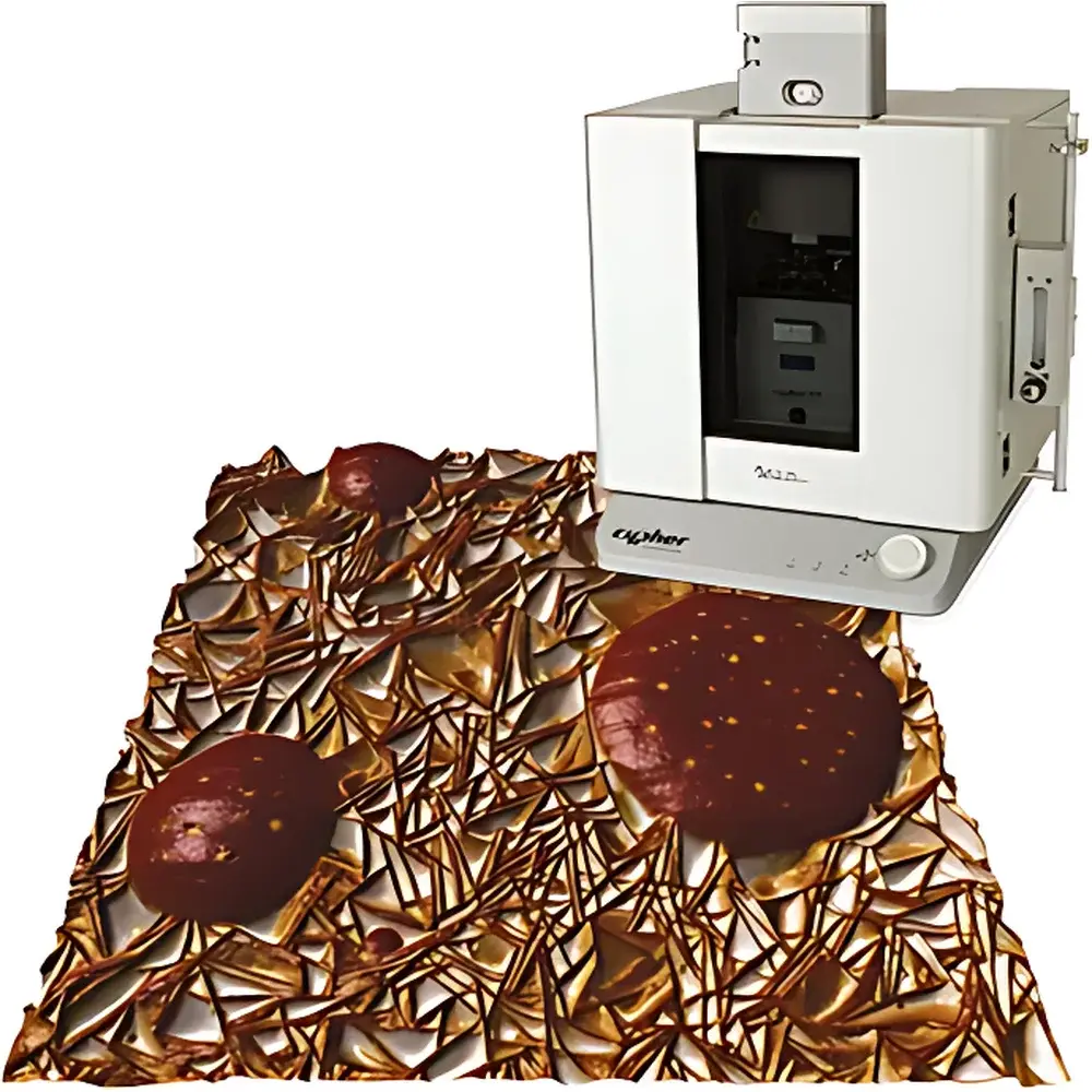
| Brand | Oxford Instruments |
|---|---|
| Origin | USA |
| Manufacturer Type | Authorized Distributor |
| Origin Category | Imported |
| Model | Cypher ES Polymer Edition |
| Price Range | USD 420,000 – 700,000 (est.) |
| Instrument Type | Atomic Force Microscope (AFM) |
| Application Class | Materials Science |
| Position Detection Noise | 625 Hz |
| Sample Dimensions | Ø < 15 mm, Thickness < 5 mm |
| Stage Travel Range | 180 mm × 180 mm |
| Environmental Control | Sealed fluid/gas chamber compatible |
| Temperature Control Range | 0–250 °C |
| Nanomechanical Capabilities | Integrated NanoMechPro toolkit (Force Modulation, Contact Resonance, and HarmoniX™) |
| Excitation Method | blueDrive photothermal excitation for tapping mode |
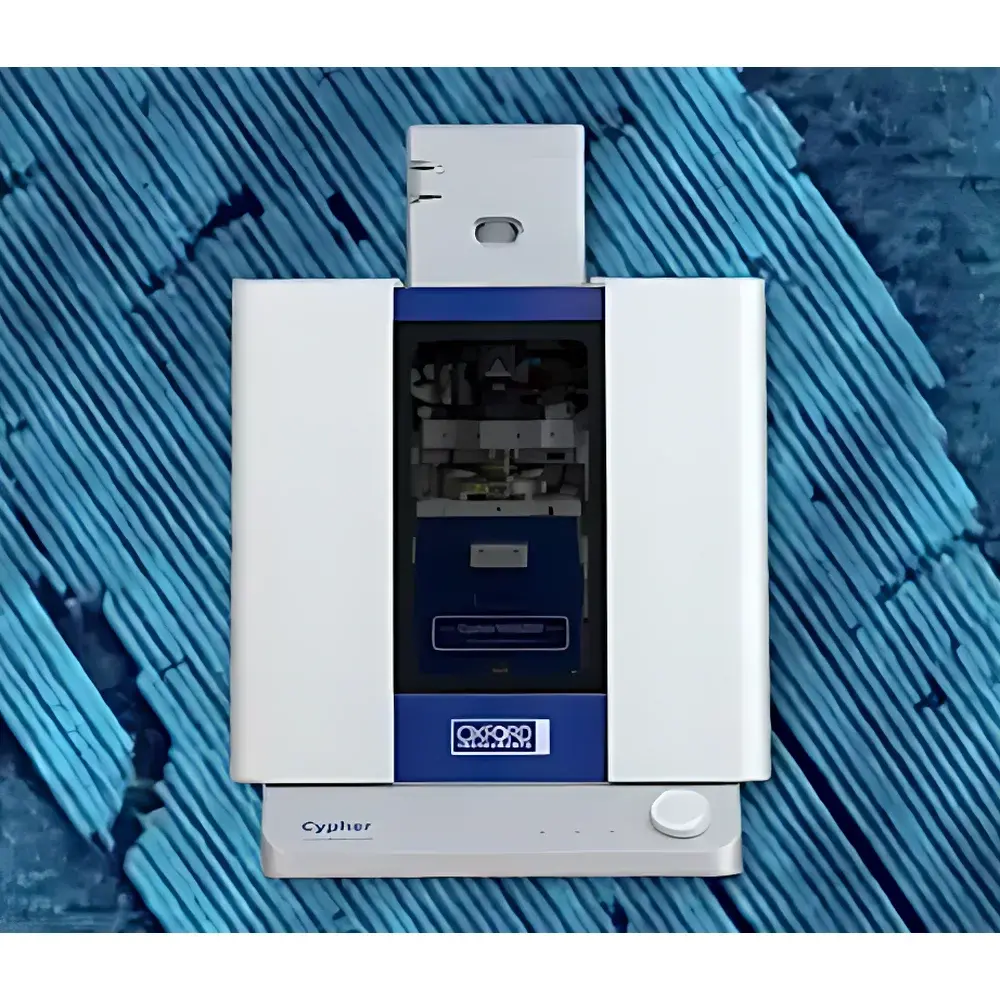
| Brand | Oxford Instruments |
|---|---|
| Origin | United Kingdom |
| Manufacturer Type | Authorized Distributor |
| Product Origin | Imported |
| Model | Cypher VRS1250 |
| Instrument Type | Materials-Focused Atomic Force Microscope |
| Position Detection Noise | X&Y < 60 pm |
| Sample Dimensions | Ø ≤ 15 mm, Thickness ≤ 7 mm |
| Stage Travel Range | 180 mm × 180 mm |
| Software | SmartScan |
| Environmental Compatibility | Fully compatible with Cypher ES environmental control system (temperature-controlled sample stage: –30 °C to +250 °C) |
| Excitation Method | blueDrive™ photothermal excitation |
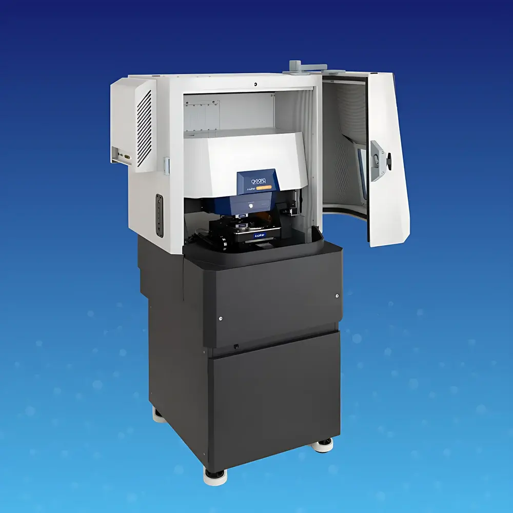
| Brand | Oxford Instruments |
|---|---|
| Origin | United Kingdom |
| Manufacturer Type | Authorized Distributor |
| Origin Category | Imported |
| Model | Jupiter Discovery AFM |
| Pricing | Available Upon Request |
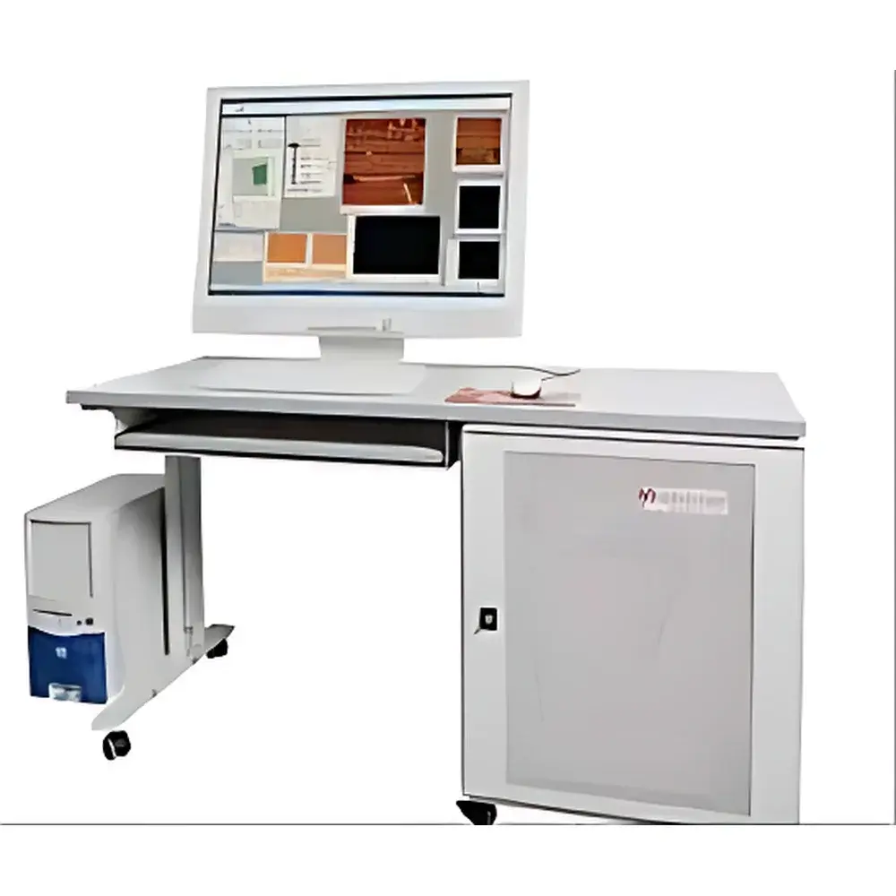
| Brand | Oxford Instruments |
|---|---|
| Origin | Germany |
| Manufacturer Type | Authorized Distributor |
| Origin Category | Imported |
| Model | Matrix |
| Price Range | USD 320,000 – 385,000 |
| Instrument Type | Magnetic Force Microscope (MFM) Control System |
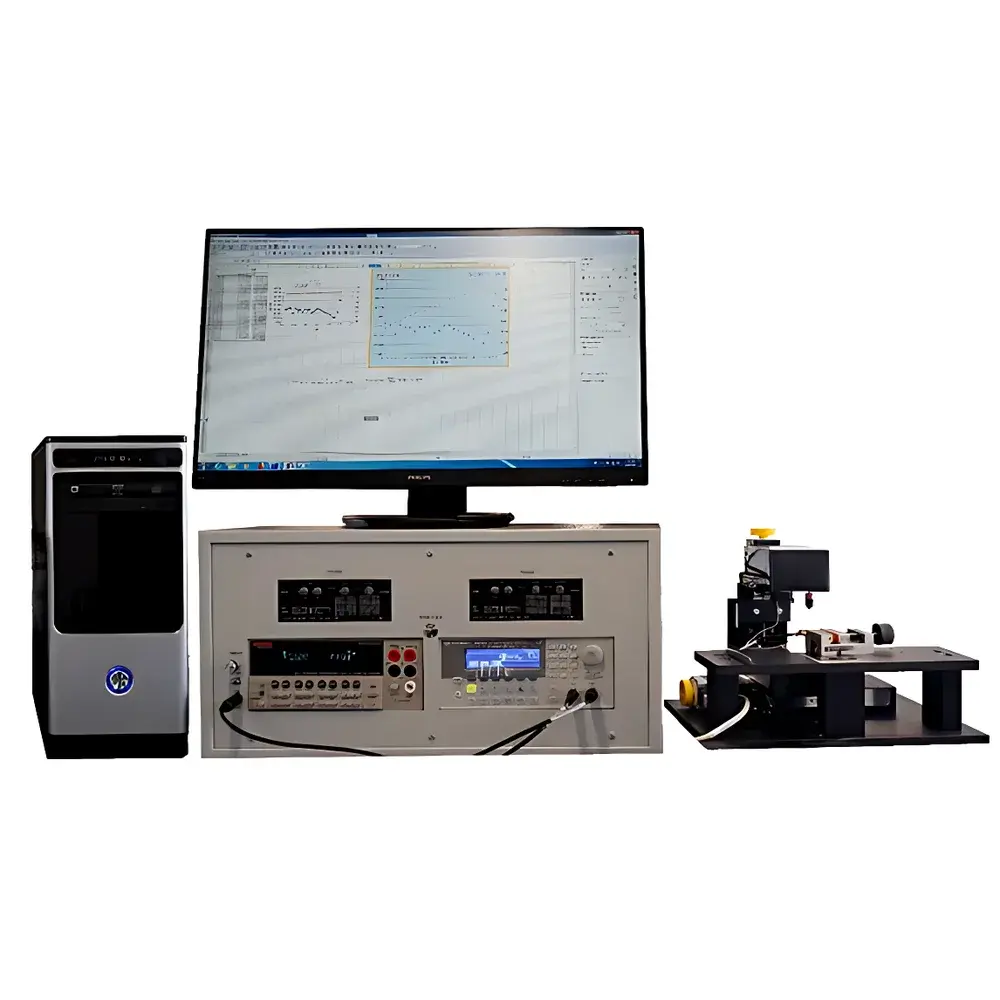
| Brand | Panco |
|---|---|
| Origin | Germany |
| Model | PSM II |
| Positioning Accuracy | Unidirectional 0.05 µm |
| Maximum Scan Area | 100 mm × 100 mm (typ.) |
| Local Measurement Resolution | 5 µm |
| Voltage Measurement Sensitivity | 100 nV |
| Seebeck Coefficient Measurement Uncertainty | < 3% (semiconductors), < 5% (metals) |
| Electrical Conductivity Measurement Uncertainty | < 4% |
| Point Acquisition Time | 4–20 s per measurement |
| Repeatability Error | < 3% |
| System Configuration | Triaxial precision positioning stage, force-sensing contact probe, integrated heating/temperature-sensing probe, analog multiplexer, 6½-digit digital voltmeter, lock-in amplifier, coaxial optical imaging module, dedicated control software with API support for LabVIEW and Python |