
Scanning Probe Microscopes
Filter
Showing 1–30 of 110 results
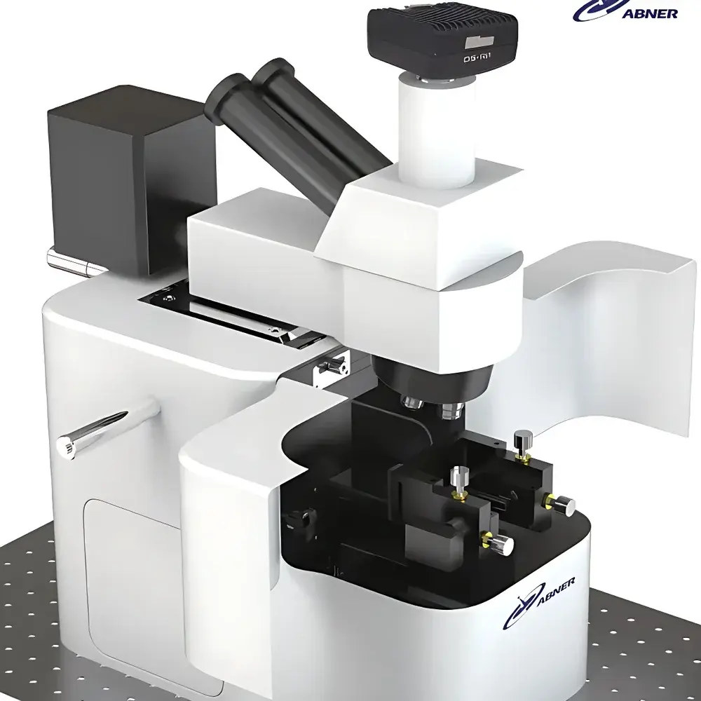
| Brand | Abner |
|---|---|
| Origin | Jiangsu, China |
| Model | ABN-AFM-001 |
| Instrument Type | Material-oriented AFM |
| Sample Dimensions | Max 15 mm × 15 mm × 2 mm |
| Scan Range | 70 µm × 70 µm (X–Y), 17 µm (Z) |
| Lateral Resolution | ≤1 nm |
| Vertical Resolution | ≤0.1 nm |
| XY Noise | ≤0.01 nm RMS |
| Z Noise | ≤0.05 nm RMS |
| Scan Speed | Up to 10 Hz |
| Probe Compatibility | Si probes with spring constants from 0.01 N/m to 40 N/m |
| Scanner | High-precision closed-loop piezoelectric scanner |
| Environmental Requirements | 18–25 °C, ≤60% RH |
| Image Resolution | 512×512 to 2048×2048 pixels |
| Interface | USB and Ethernet |
| Power Supply | 220 V/50 Hz or 110 V/60 Hz |
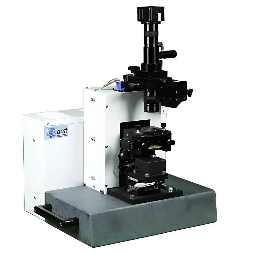
| Brand | ACST |
|---|---|
| Origin | USA |
| Manufacturer Type | Authorized Distributor |
| Origin Category | Imported |
| Model | ACST-AFM |
| Instrument Type | Biological AFM |
| Position Detection Noise | ≤0.15 nm RMS |
| Maximum Sample Size | 15 mm diameter |
| XY Stage Travel Range | 25 mm × 25 mm |
| Software | Aotu AFM |
| Imaging Modes | Contact, Tapping, Phase, Lateral Force, Advanced Force Spectroscopy, Conductive AFM, Magnetic AFM, Nanolithography |
| XY Scanner Range | >50 µm (closed-loop), <10 nm resolution (closed-loop), <1 nm resolution (open-loop) |
| Z Scanner Range | >16 µm |
| Z Sensor Noise | <5 nm |
| Z Feedback Noise | <0.2 nm |
| Z Actuation | Direct-drive stepper motor, 25 mm travel, 330 nm minimum step, 8 mm/min max speed |
| Optical System | 3 MP CCD camera, 45×–400× real-time magnification |
| Base Material | Solid granite for vibration isolation and mechanical stability |
| Probe Loading | Tool-free, rapid exchange design |
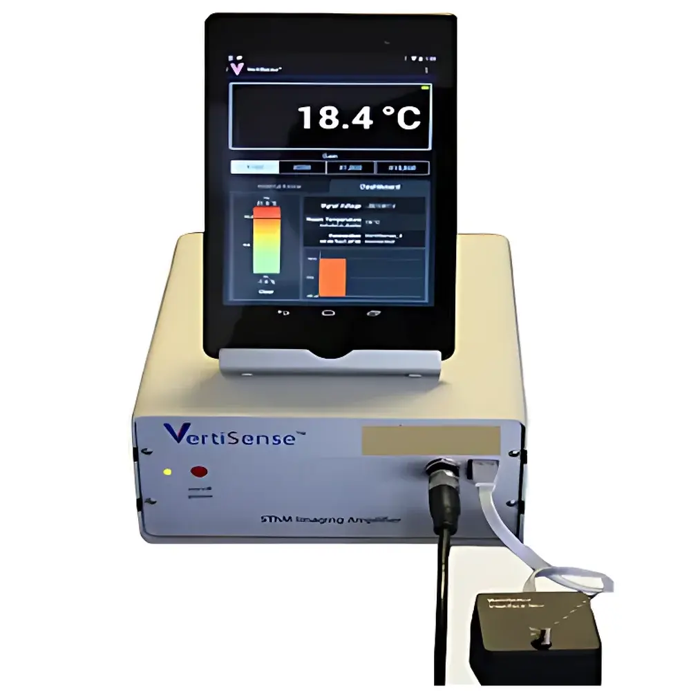
| Brand | AppNano |
|---|---|
| Origin | USA |
| Manufacturer Type | Authorized Distributor |
| Product Category | Imported Instrument |
| Model | VertiSense |
| Instrument Type | Material Science AFM-Compatible SThM Module |
| Primary Function | Nanoscale Thermal Property Mapping (Topography + Thermal Conductivity + Temperature Distribution) |
| Origin | USA |
|---|---|
| Manufacturer Type | Distributor |
| Origin Category | Imported |
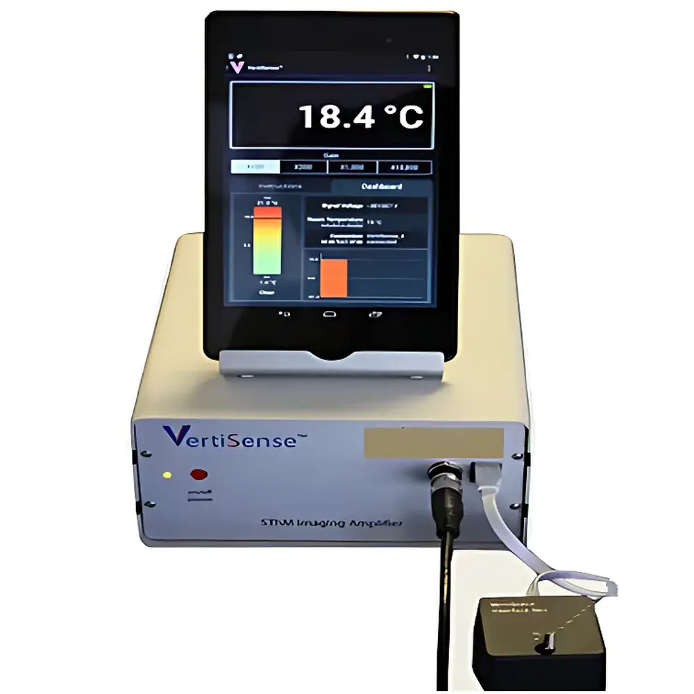
| Model | VertiSense |
| Price Range | USD 14,000 – 72,000 (based on AFM integration configuration) |
| Instrument Type | Atomic Force Microscope (AFM)-Compatible Thermal Scanning Probe Module |
| Temperature Resolution | ≤ 10 mK (dependent on host AFM electronics and thermal calibration) |
| Spatial Thermal Resolution | ≤ 20 nm (tip-limited, under optimal vacuum/low-noise conditions) |
| Maximum Tip Operating Temperature | 700 °C |
| Sample Stage Compatibility | Fully compatible with standard commercial AFM sample stages (e.g., Bruker Dimension, Keysight 5500, Park Systems XE-series, Nanosurf Flex-Axiom) |
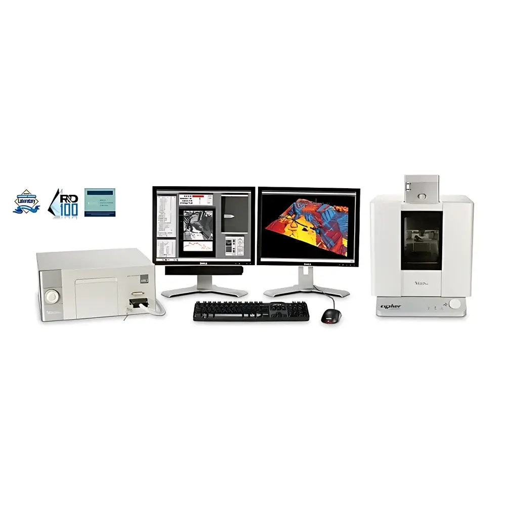
| Brand | Oxford Instruments |
|---|---|
| Origin | Germany |
| Manufacturer Type | Authorized Distributor |
| Origin Category | Imported |
| Model | GetReal |
| Price Range | USD 13,500 – 68,000 |
| Instrument Type | AFM Calibration Module |
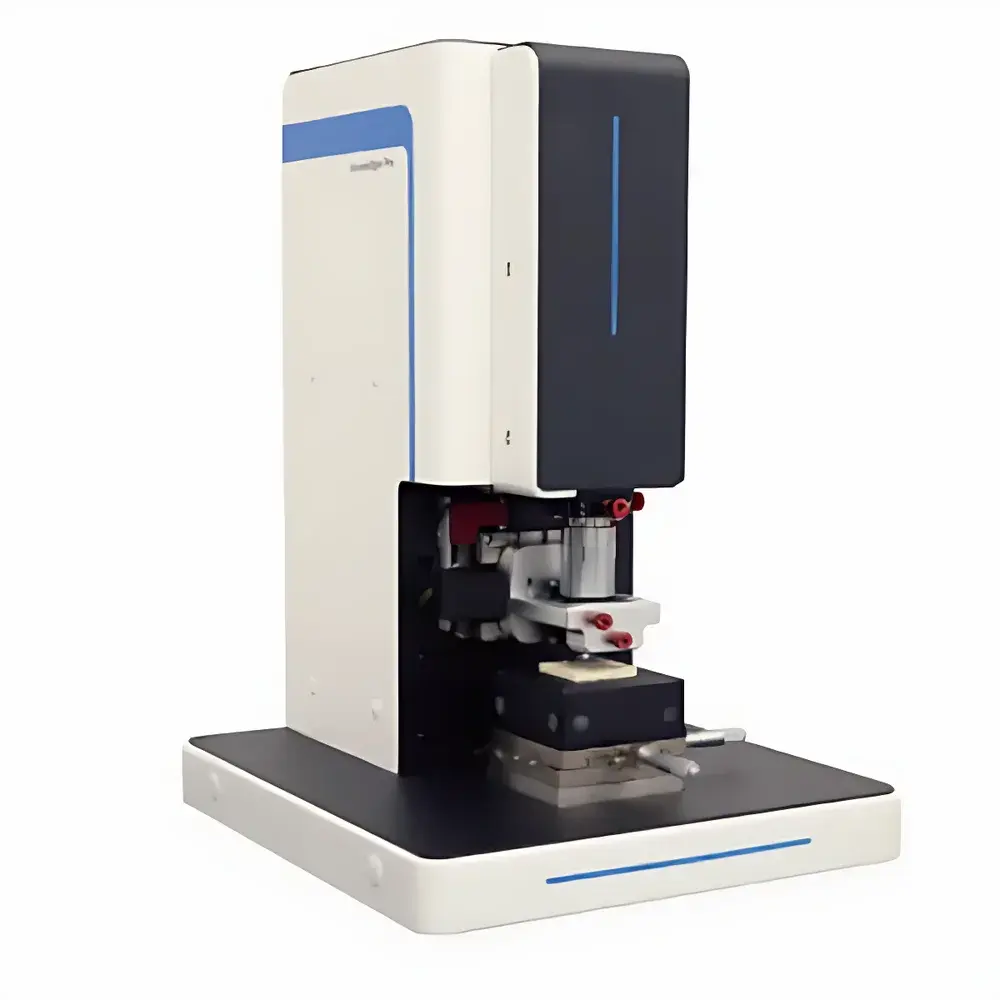
| Brand | Truth Instruments Company Limited |
|---|---|
| Origin | Beijing, China |
| Manufacturer Type | Authorized Distributor |
| Country of Origin | China |
| Model | AtomEdge Pro |
| Pricing | Available Upon Request |
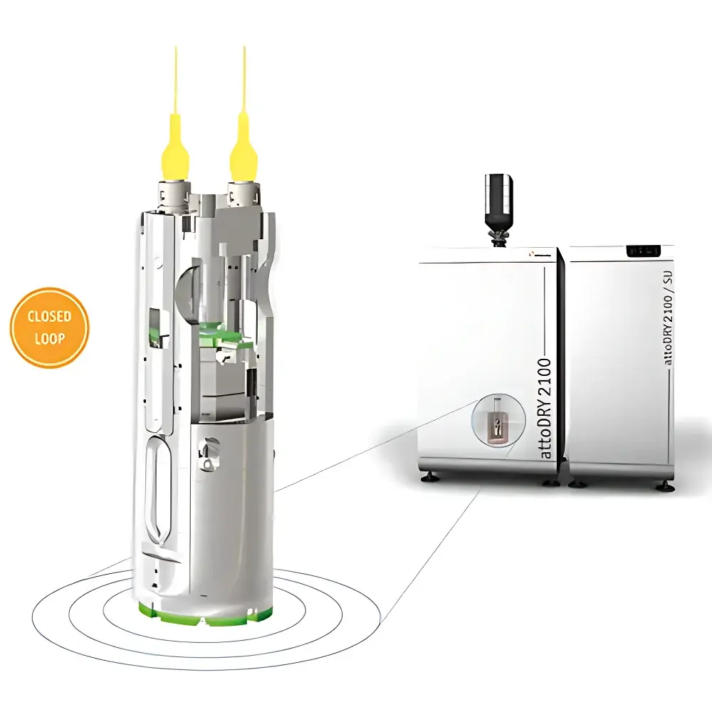
| Brand | attocube |
|---|---|
| Origin | Germany |
| Model | attoCFM I |
| Instrument Type | Cryogenic Confocal Microscope for Quantum Materials Research |
| Positioning Noise | < 0.5 nm |
| Sample Size Capacity | Ø100 mm |
| Sample Stage Travel Range | 150 µm (fine scan) / 5 × 5 × 5 mm³ (coarse positioning) |
| Temperature Range | 1.8 K – 300 K |
| Magnetic Field | Up to 12 T (vector magnet optional) |
| Vacuum Operating Range | 1 × 10⁻⁶ mbar – 1 atm |
| Optical Resolution | ~550 nm (at 635 nm, NA = 0.82) |
| Scan Area | 30 × 30 µm² @ 4 K |
| Objective | Cryo-optimized Achromatic Objective, NA = 0.82, WD = 0.7 mm |
| Expandable Modules | AFM/MFM/PFM/KPFM/ct-AFM/cryo-Raman |
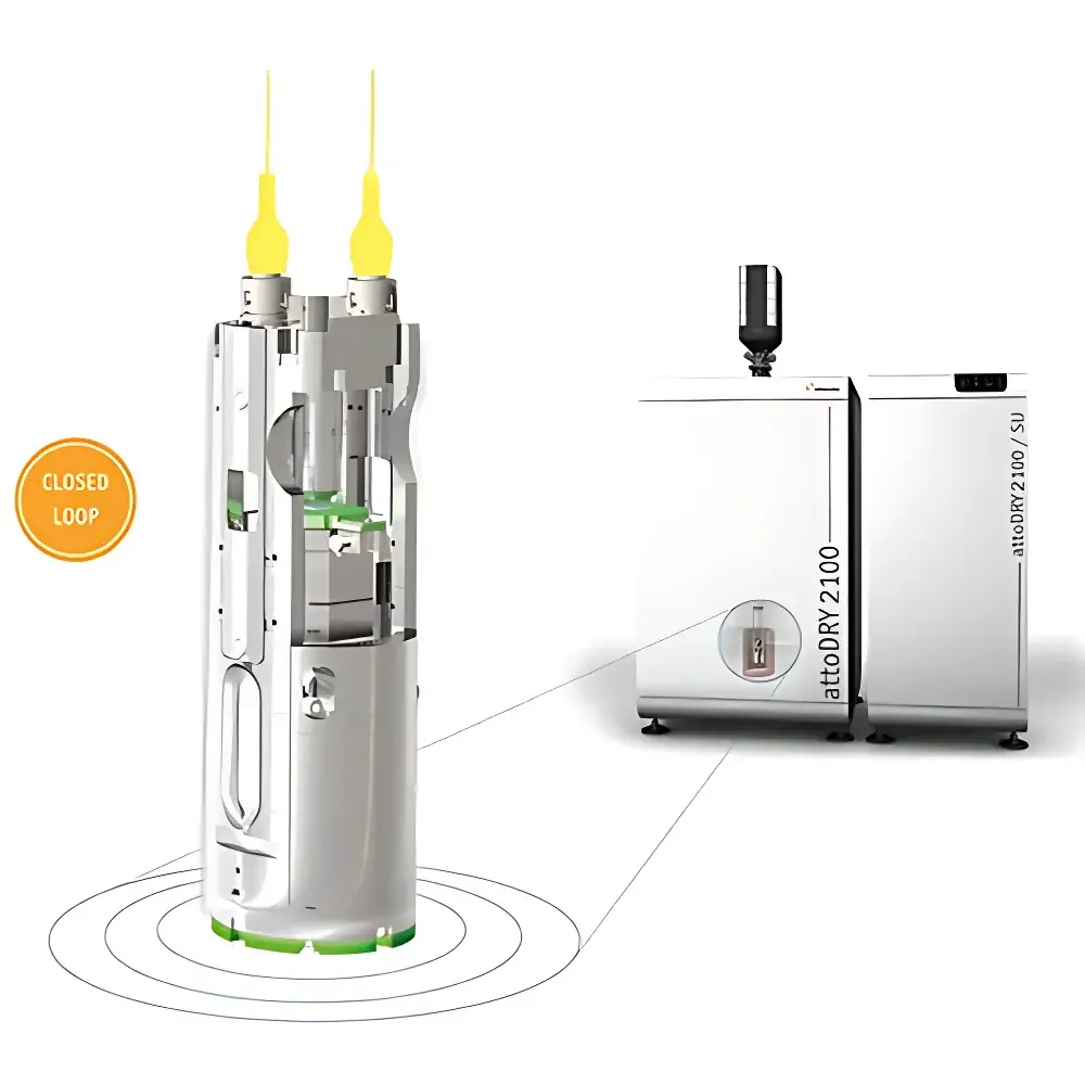
| Brand | attocube |
|---|---|
| Origin | Germany |
| Model | attoCFM I |
| Instrument Type | Magnetic Force Microscope (MFM) / Cryogenic Confocal Microscope |
| Positioning Noise | < 0.5 nm |
| Sample Size Capacity | Ø100 mm |
| Sample Stage Travel Range | 150 µm (fine scan) / 5 × 5 × 5 mm³ (coarse positioning) |
| Temperature Range | 1.8 K – 300 K |
| Magnetic Field | Up to 12 T (vector magnet optional) |
| Vacuum Operation | 1 × 10⁻⁶ mbar – 1 atm |
| Numerical Aperture (NA) | 0.82 |
| Optical Resolution | ~550 nm (@635 nm) |
| Working Distance (WD) | 0.7 mm |
| Confocal Scan Range | 30 × 30 µm² @4 K |
| Compatible Cryostats | attoDRY1000/2100, Quantum Design PPMS (1″/2″ bore) |
| Expandable Modules | AFM/MFM/PFM/KPFM/ct-AFM/cryo-Raman |
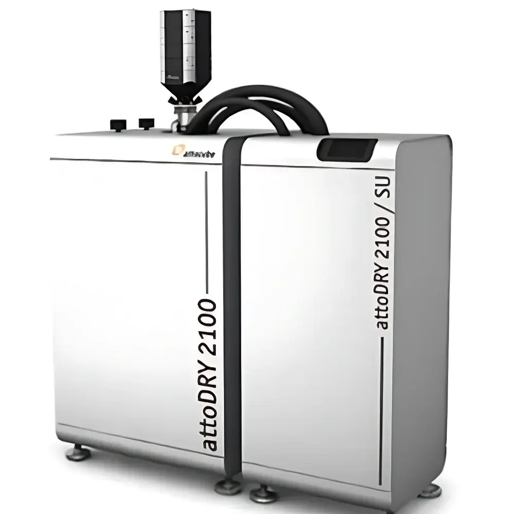
| Brand | Attocube Systems AG |
|---|---|
| Origin | Germany (manufactured in Germany |
| Instrument Type | Research-grade industrial SPM platform |
| Magnet Strength | Up to 15 T |
| Temperature Range | 1.5 K – 300 K (continuous, closed-cycle) |
| Positioning Noise | < 0.5 nm RMS |
| Sample Dimensions | Max 100 mm × 50 mm × 20 mm |
| XY Scanner Range | 10 µm × 10 µm |
| Vibration Level | 0.12 nm RMS (typical) |
| Compliance | ASTM E2579, ISO/IEC 17025 compatible operation environment |
| Software Control | Integrated touchscreen interface with automated temperature/magnetic field ramping |
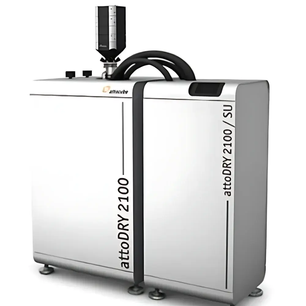
| Brand | Attocube Systems AG |
|---|---|
| Origin | Germany |
| Model | attoDRY Lab |
| Instrument Type | Cryogenic Scanning Probe Microscope (SPM) |
| Magnetic Field Strength | Up to 15 T |
| Temperature Range | 1.5 K – 300 K (closed-cycle) |
| Positioning Noise | < 0.5 nm RMS |
| Sample Dimensions | Max 100 mm × 50 mm × 20 mm |
| XY Scanner Range | 10 µm × 10 µm |
| Vibration Level | 0.12 nm RMS (typ.) |
| Compliance | ASTM E2917, ISO/IEC 17025 compatible workflows, GLP/GMP-ready data logging |
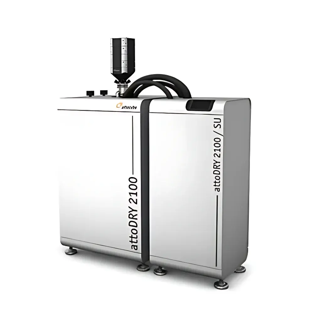
| Brand | Attocube Systems AG |
|---|---|
| Origin | Germany |
| Model | attoDRY Lab |
| Instrument Type | Magnetic Force Microscope (MFM) |
| Positioning Noise | 0.12 nm RMS |
| Sample Stage Travel Range | 5 mm × 5 mm × 5 mm |
| Temperature Range | 1.5 K – 300 K (configurable) |
| Maximum Magnetic Field | 15 T |
| Cooling Time (to base temperature) | ~1–2 hours |
| Control Interface | Integrated touchscreen with automated thermal and magnetic field sequencing |
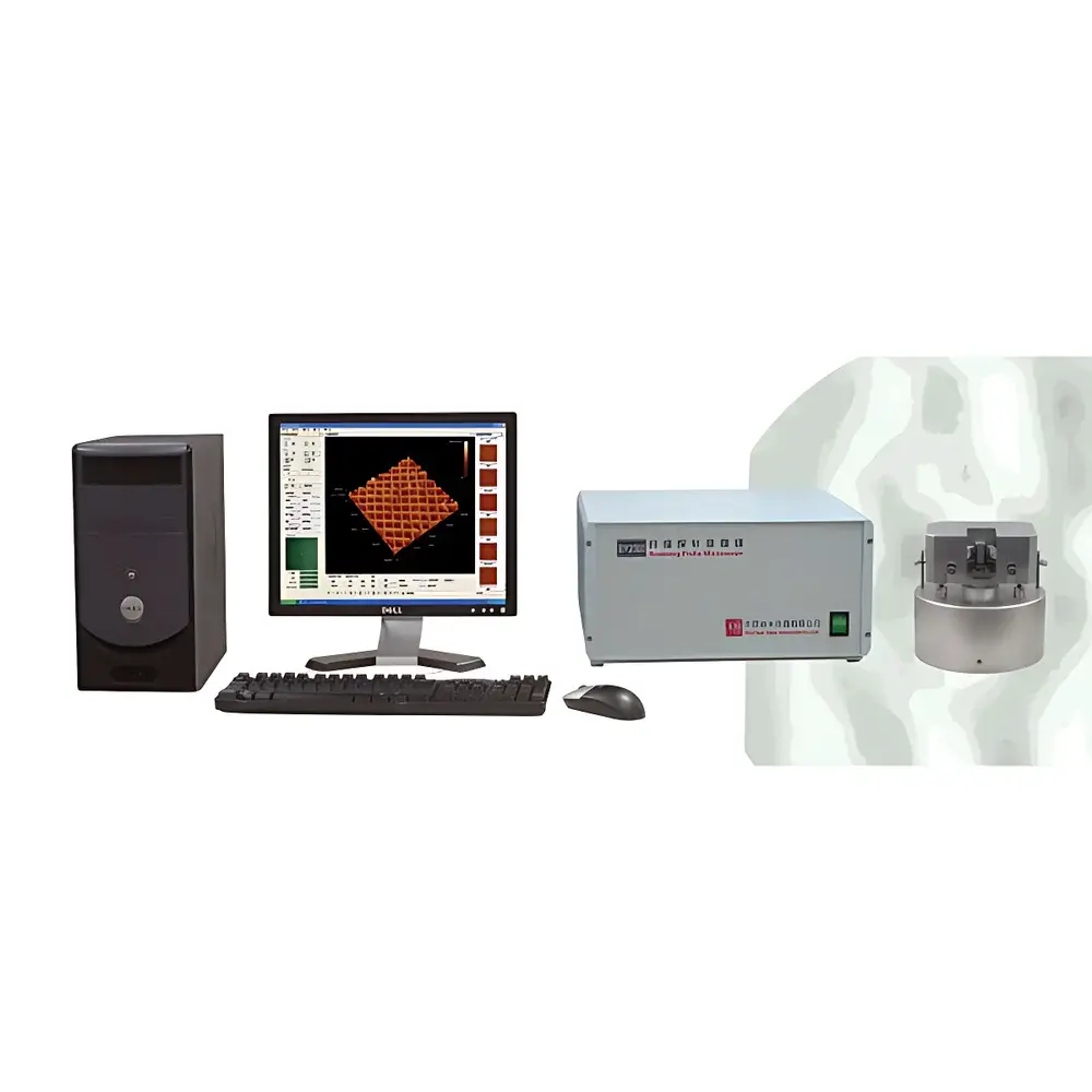
| Brand | Benyuan Nano |
|---|---|
| Origin | Beijing, China |
| Manufacturer Type | Authorized Distributor |
| Product Origin | Domestic (China) |
| Model | BY1000 |
| Price Range | USD 14,000 – 70,000 |
| Instrument Type | Scanning Tunneling Microscope (STM) |
| Position Detection Noise | 0.1 Å RMS |
| Maximum Sample Size | Ø45 mm × 15 mm |
| XY Sample Stage Travel Range | 100 mm × 100 mm |
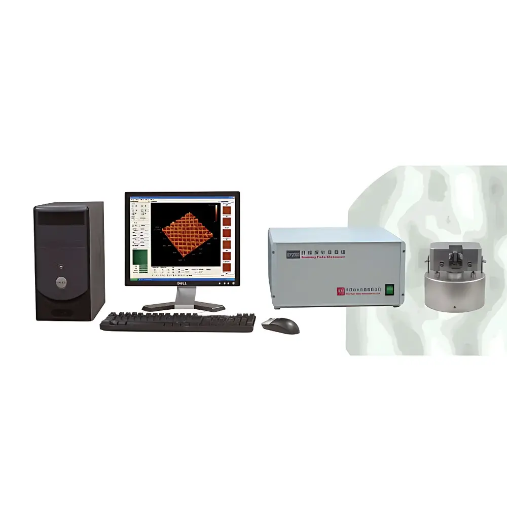
| Brand | Benyuan Nano |
|---|---|
| Origin | Beijing, China |
| Manufacturer Type | Authorized Distributor |
| Country of Origin | China |
| Model | BY3000 |
| Price Range | USD 14,000 – 72,000 |
| Instrument Type | Atomic Force Microscope (AFM) |
| Position Detection Noise | 0.1 nm |
| Maximum Sample Diameter | 45 mm |
| Maximum Sample Thickness | 15 mm |
| XY Sample Stage Travel Range | 100 mm × 100 mm |
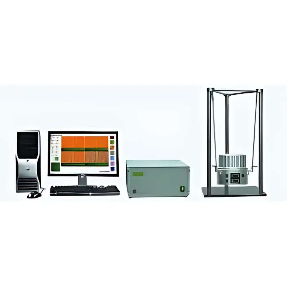
| Brand | BENYUAN Nano |
|---|---|
| Model | CSPM5500 |
| Origin | Beijing, China |
| Instrument Type | Atomic Force Microscope (AFM) with integrated Scanning Tunneling Microscope (STM) and Lateral Force Microscope (LFM) |
| Position Detection Noise | 0.1 nm |
| Sample Diameter Limit | <102 mm (4 in) |
| Sample Thickness Limit | <40 mm |
| XY Sample Stage Travel Range | 100 mm × 100 mm |
| Maximum Z-Travel (Auto-Approach) | >30 mm |
| Image Resolution | Up to 4096 × 4096 physical pixels |
| Horizontal Resolution (AFM) | 0.2 nm (mica-calibrated) |
| Vertical Resolution (AFM) | 0.1 nm (mica-calibrated) |
| Horizontal Resolution (STM) | 0.1 nm (graphite-calibrated) |
| Vertical Resolution (STM) | 0.01 nm (graphite-calibrated) |
| Data Interface | Fast Ethernet (10/100 Mbps) or USB 2.0 |
| Real-Time 3D Visualization | Yes |
| PID-Controlled Force Feedback | Yes |
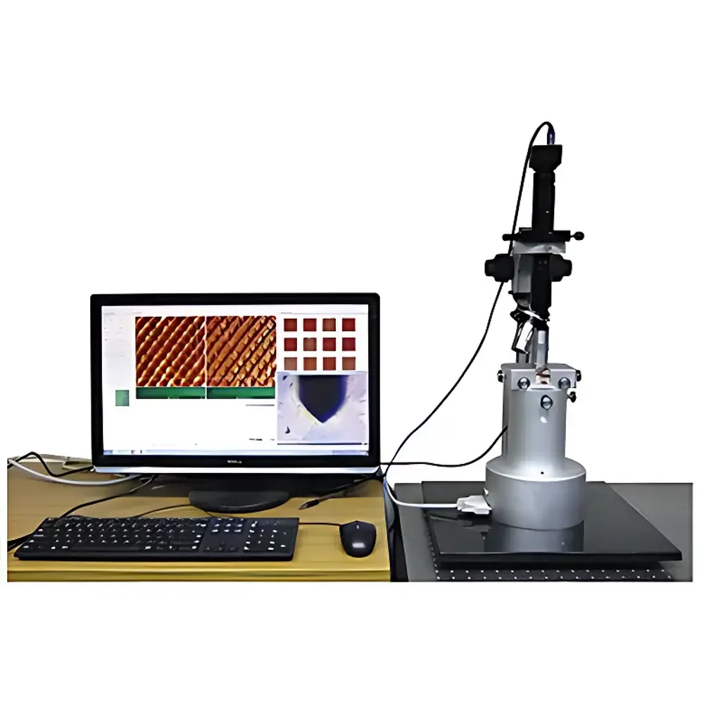
| Brand | Betop Scientific |
|---|---|
| Origin | Guangdong, China |
| Manufacturer Type | OEM Manufacturer |
| Country of Origin | China |
| Model | CSPM6000 |
| Instrument Type | Atomic Force Microscope (AFM) |
| Position Detection Noise | ≤0.1 nm |
| Sample Dimensions | Ø < 100 mm, Thickness < 40 mm |
| XY Sample Stage Travel Range | 100 mm × 100 mm |
| Force Sensitivity | ≤5 pN |
| Image Resolution Options | 128×128 to 4096×4096 pixels |
| Scan Rotation | 0–360° |
| Scan Frequency Range | 0.1–100 Hz |
| Control Architecture | Dual-core DSP+ARM processor (Texas Instruments) |
| Feedback System | Fully digital PID-controlled feedback with auto-tuning |
| Communication Interfaces | Gigabit Ethernet (TCP/IP) + High-Speed USB 2.0 |
| Display | 16×4 LCD with real-time system diagnostics |
| Software | Multi-language (EN/CN-Traditional/CN-Simplified), Windows 10/7/XP/Vista compatible |
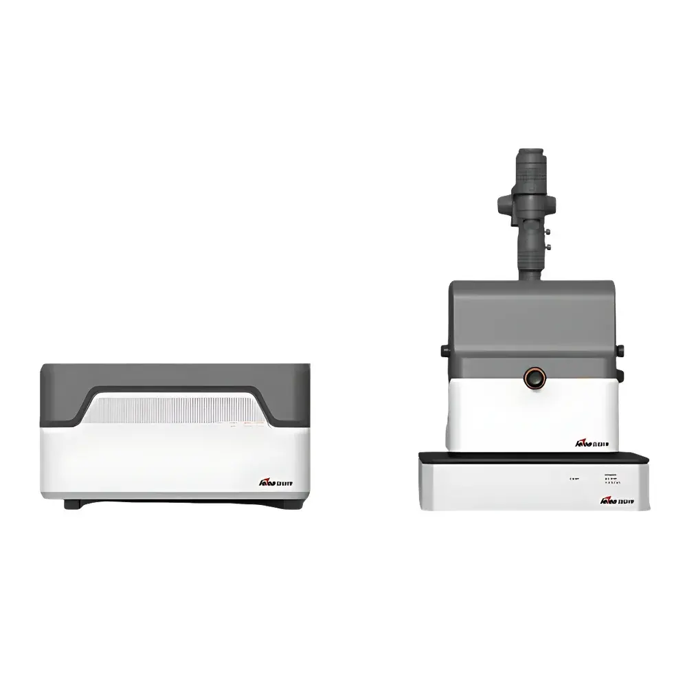
| Brand | Betop Scientific |
|---|---|
| Origin | Beijing, China |
| Manufacturer Type | Original Equipment Manufacturer (OEM) |
| Country of Origin | China |
| Model | OpenSPM |
| Instrument Category | Atomic Force Microscope (AFM) |
| Instrument Type | Materials Science AFM |
| Z-Direction Position Detection Noise (RMS) | ≤0.05 nm (calibrated on monolayer step height of HOPG graphite) |
| Maximum Sample Diameter | ≤30 mm |
| Maximum Sample Thickness | ≤20 mm |
| Sample Stage Travel Range (Auto-Approach) | ≥23 mm (one-click automated approach), Minimum Step Resolution: ≤50 nm |
| Manual XY Adjustment Range | ≥±8.0 mm |
| Scanner Type | Tube Scanner |
| Maximum Scan Range | ≥20 μm × 20 μm × 3 μm |
| Lateral Resolution | <0.02 nm (in-plane) |
| Scan Rate | 0.1–30 lines/sec |
| PID Feedback Loop Response Time | <10 μs |
| Max Pixel Density per Image | 4000 × 4000 physical pixels |
| Real-Time Simultaneous Data Channels | ≥5 |
| Control Architecture | Dual-Core Embedded System (ARM + DSP) |
| Communication Protocol | TCP/IP |
| Detection Mode | Frequency Modulation (FM-AFM) with Integrated Analog-Digital Lock-in Amplifier |
| Software Capabilities | Real-time 3D surface rendering, multi-parameter mapping (topography, phase, friction, current, force-distance, I–V, I–Z), tip characterization & image deconvolution algorithms |
| Compliance | Designed for GLP-compliant materials characterization workflows |
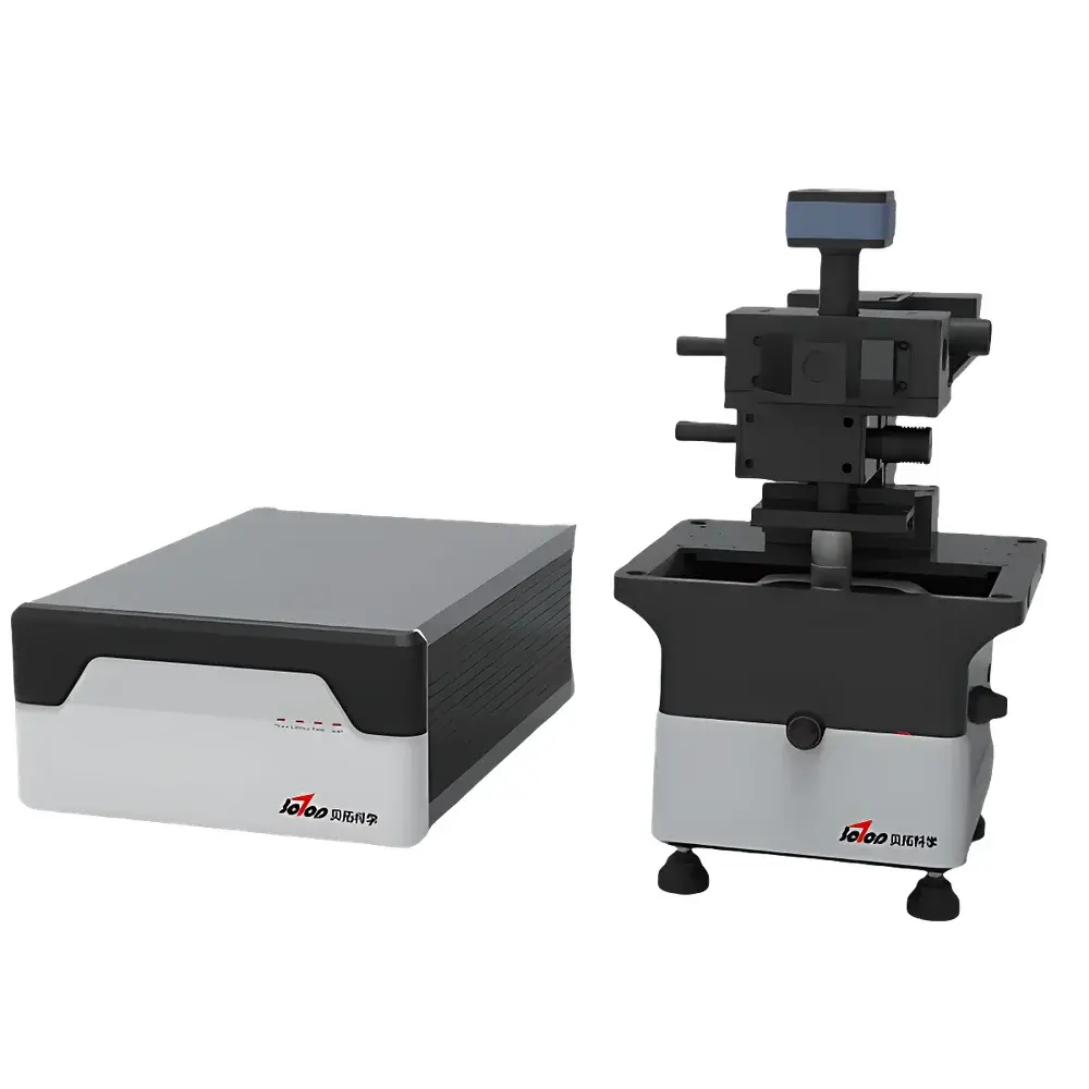
| Brand | Betop Scientific |
|---|---|
| Origin | Guangdong, China |
| Manufacturer Type | Original Equipment Manufacturer (OEM) |
| Country of Origin | China |
| Model | RamSPM |
| Price Range | USD 70,000 – 140,000 |
| Instrument Category | Atomic Force Microscope (AFM) |
| Instrument Class | Materials Science AFM |
| Z-direction RMS System Noise | ≤0.05 nm (calibrated on monolayer step height of HOPG) |
| Maximum Sample Diameter | ≤30 mm |
| Maximum Sample Thickness | ≤20 mm |
| Auto-approach Travel Range | ≥23 mm |
| Minimum Step Resolution | ≤50 nm |
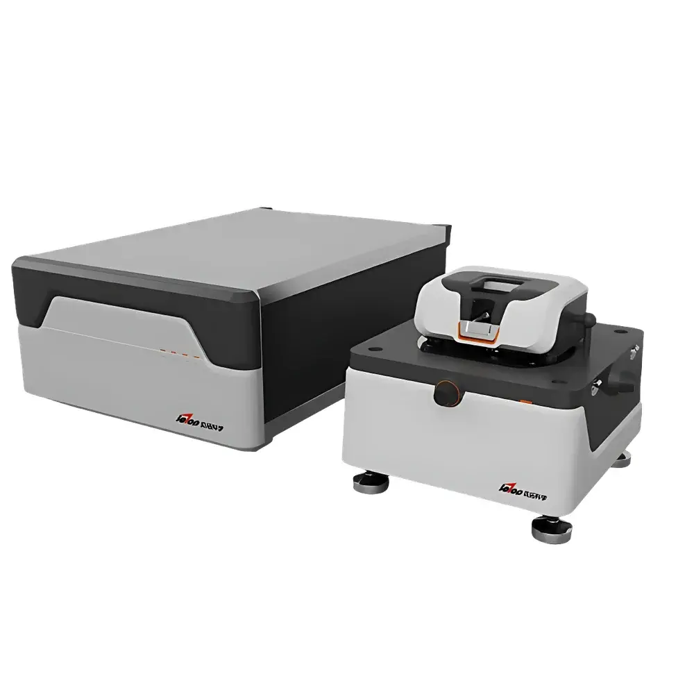
| Brand | Betop Scientific |
|---|---|
| Origin | Beijing, China |
| Manufacturer Type | Manufacturer |
| Product Category | Domestic |
| Model | TopSPM |
| Price Range | USD 84,000 – 182,000 |
| Instrument Type | Atomic Force Microscope (AFM) |
| Application Class | Materials Science AFM |
| Z-direction RMS System Noise | ≤0.05 nm (calibrated on graphite monolayer step height) |
| Maximum Sample Diameter | ≤30 mm |
| Maximum Sample Thickness | ≤20 mm |
| Auto-Approach Travel Range | ≥23 mm |
| Minimum Approach Step Resolution | ≤50 nm |
| Closed-Loop XY Scan Range | ≥30 µm × 30 µm |
| Closed-Loop Z Scan Range | ≥8 µm |
| Scan Resolution | <1.5 nm |
| Line Rate | 0.1–30 lines/sec |
| PID Feedback Response Time | <10 µs |
| Max Pixel Density per Image | 4000 × 4000 |
| Real-Time Simultaneous Data Channels | ≥5 |
| Control Architecture | Dual-Core Embedded System (ARM + DSP) |
| Communication Protocol | TCP/IP |
| Detection Mode | Frequency Modulation (FM-AFM) |
| Integrated Lock-in Amplifier | Analog-Digital Hybrid Structure |
| Probe Compatibility | Self-Sensing Probes & Conventional Laser-Detected Cantilevers |
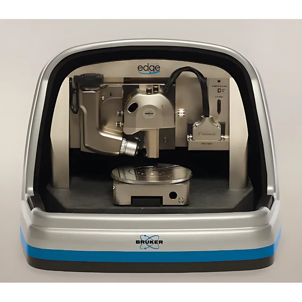
| Brand | Bruker |
|---|---|
| Origin | USA |
| Model | Dimension Edge |
| Instrument Type | Material-Focused AFM |
| Positioning Noise | X-Y ≤ 50 pm RMS, Z ≤ 50 pm RMS |
| Sample Diameter | 150 mm (vacuum chuck), Thickness: ≤ 15 mm |
| Scan Area | 150 mm × 150 mm |
| Imaging Bandwidth | Typical high-speed acquisition capability |
| Category | Scanning Probe Microscope (SPM) / Atomic Force Microscope (AFM) |
| Brand | Bruker |
|---|---|
| Origin | Malaysia |
| Manufacturer Type | Authorized Distributor |
| Origin Category | Imported Instrument |
| Model | Dimension Edge |
| Price Range | USD 135,000 – 205,000 (FOB) |
| Instrument Type | Atomic Force Microscope (AFM) |
| Positional Noise (X-Y, Closed-Loop) | ≤0.15 nm RMS at standard imaging bandwidth (up to 625 Hz) |
| Z-Noise (Closed-Loop) | 35 pm RMS at standard imaging bandwidth (up to 625 Hz) |
| Sample Diameter Capacity | 210 mm |
| XY Stage Travel Range | 150 mm × 150 mm |
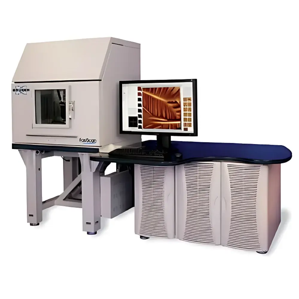
| Brand | Bruker |
|---|---|
| Origin | USA |
| Manufacturer Type | Authorized Distributor |
| Origin Category | Imported Instrument |
| Model | Dimension FastScan |
| Instrument Type | Materials-Focused AFM |
| Position Detection Noise | X-Y ≤ 0.15 nm RMS, Z = 35 pm RMS |
| Typical Imaging Bandwidth | Up to 625 Hz |
| Sample Diameter | 210 mm (vacuum chuck), Max Thickness: ≤ 15 mm |
| Stage Travel Range | 180 mm × 150 mm |
| Brand | Bruker |
|---|---|
| Origin | Germany |
| Model | Dimension FastScan |
| Instrument Type | Materials-Focused AFM |
| XY Positioning Noise | ≤0.15 nm |
| Sample Dimensions | Ø ≤ 15 mm, Thickness ≤ 5 mm |
| Stage Travel Range | 180 mm × 180 mm |
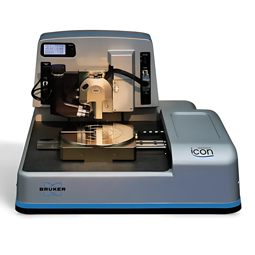
| Brand | Bruker |
|---|---|
| Origin | Germany |
| Manufacturer Type | Authorized Distributor |
| Origin Category | Imported |
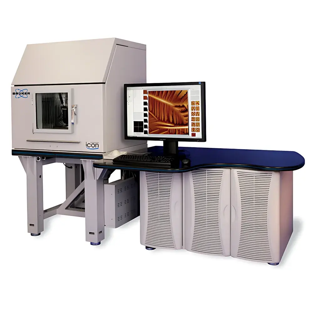
| Model | Dimension Icon |
| Price Range | USD 135,000 – 205,000 (est.) |
| Instrument Type | Atomic Force Microscope |
| Application Class | Materials Science AFM |
| Position Detection Noise | <0.15 nm RMS (at typical imaging bandwidth up to 625 Hz) |
| Sample Diameter | Up to 210 mm |
| Sample Thickness Limit | ≤5 mm |
| XY Stage Travel Range | 180 mm × 150 mm |
| XY Repeatability | 2 µm (unidirectional), 3 µm (bidirectional) |
| Brand | Bruker |
|---|---|
| Origin | Malaysia |
| Manufacturer Type | Authorized Distributor |
| Origin Category | Imported |
| Model | Dimension Icon |
| Instrument Type | Atomic Force Microscope |
| X-Y Positioning Noise (Closed-Loop) | ≤0.15 nm RMS (Standard Imaging Bandwidth, up to 625 Hz) |
| Z Positioning Noise (Closed-Loop) | 35 pm RMS (Standard Imaging Bandwidth, up to 625 Hz) |
| Maximum Sample Diameter | 210 mm |
| Sample Stage Travel Range | 150 mm |
| Brand | Bruker |
|---|---|
| Origin | USA |
| Model | Dimension Icon |
| Instrument Type | Atomic Force Microscope (AFM) |
| Vertical Noise Floor (Z-sensor, closed-loop) | <35 pm RMS |
| Typical Imaging Bandwidth | 625 Hz |
| Sample Stage | 210 mm vacuum chuck (Ø210 mm × 15 mm thick) |
| Stage Travel Range (X-Y visual field) | 180 mm × 180 mm |
| X-Y Scan Range (typical) | 90 µm × 90 µm |
| Z Scan Range (typical) | 10 µm |
| X-Y Positioning Noise (closed-loop) | <0.15 nm RMS (625 Hz) |
| Z Sensor Noise (closed-loop) | <35 pm RMS (625 Hz) |
| Overall Linearity Error (X-Y-Z) | 0.5% (typical) |
| Optical System | 5 MP digital camera, 180–1465 µm field of view, digital zoom & auto-focus |
| Controller | NanoScope V |
| Integrated Vibration Isolation | Monolithic pneumatic isolation table |
| Acoustic Enclosure | Rated for continuous ambient noise up to 85 dBC |
| Brand | Bruker |
|---|---|
| Origin | USA |
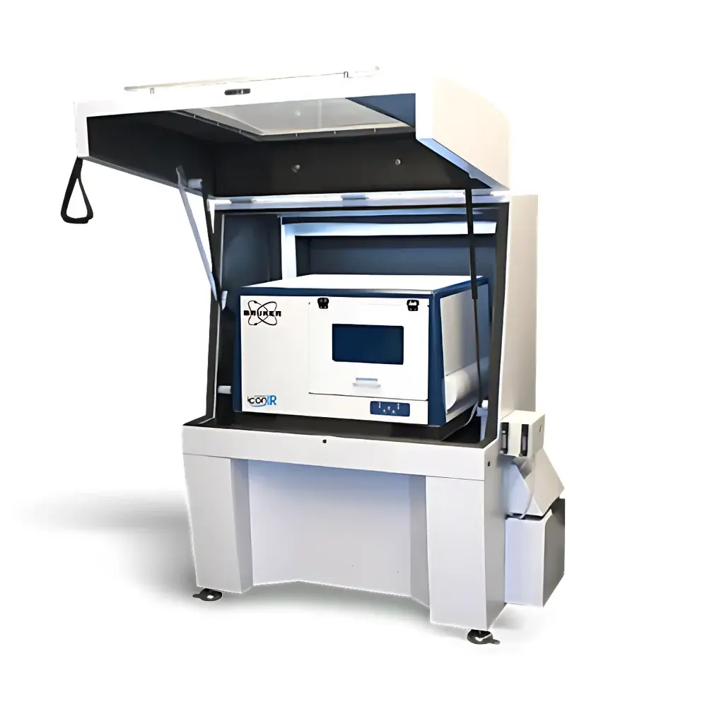
| Model | Dimension IconIR |
| Type | Modular Scanning Probe Microscope (SPM) with Integrated AFM-IR |
| Measurement Principle | Photothermal Induced Resonance (PTIR) / Nanoscale Fourier Transform Infrared (nano-FTIR) |
| Spatial Resolution | <10 nm |
| Sensitivity | Monolayer-level chemical detection |
| Compatibility | PeakForce Tapping® for nanomechanical & nanoelectrical correlative mapping |
| Software Platform | NanoScope Analysis with IR spectral library integration |
| Compliance | Supports GLP/GMP audit trails, ASTM E2987 (for nanoscale spectroscopic imaging), ISO/IEC 17025 traceability frameworks |
| Brand | Bruker |
|---|---|
| Origin | USA |
| Manufacturer Type | Authorized Distributor |
| Origin Category | Imported |
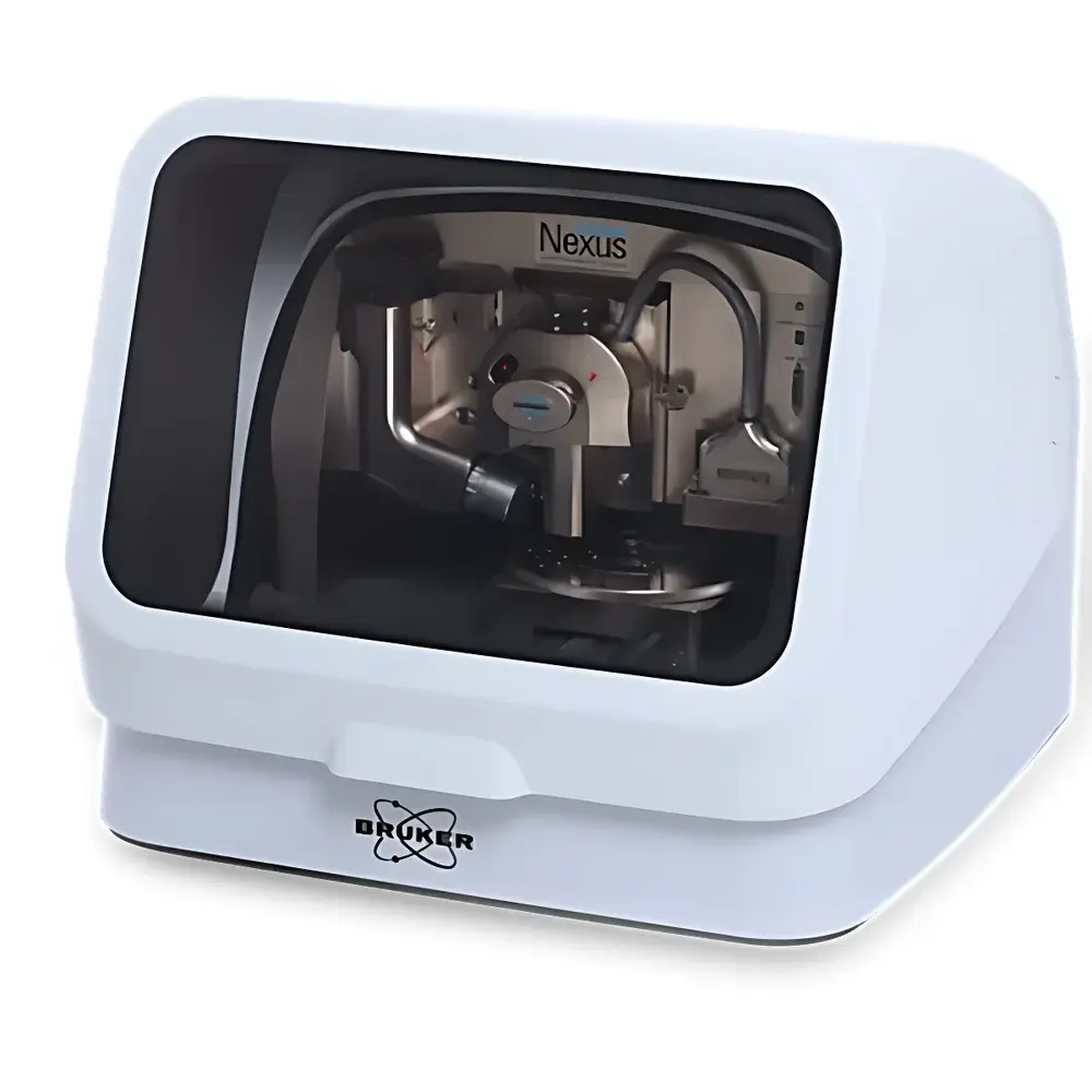
| Model | Dimension Nexus |
| Instrument Type | Atomic Force Microscope |
| Application Class | Materials Science AFM |
| Architecture | Modular, Multi-Mode Scanning Probe Microscope |
| Controller Platform | NanoScope 6 |
| Core Imaging Modes | PeakForce Tapping®, PeakForce QNM®, PeakForce MFM®, ScanAsyst® Auto-Optimization |
| Environmental Operation | Air, Liquid, Controlled Atmosphere |
| Brand | Bruker |
|---|---|
| Origin | USA |
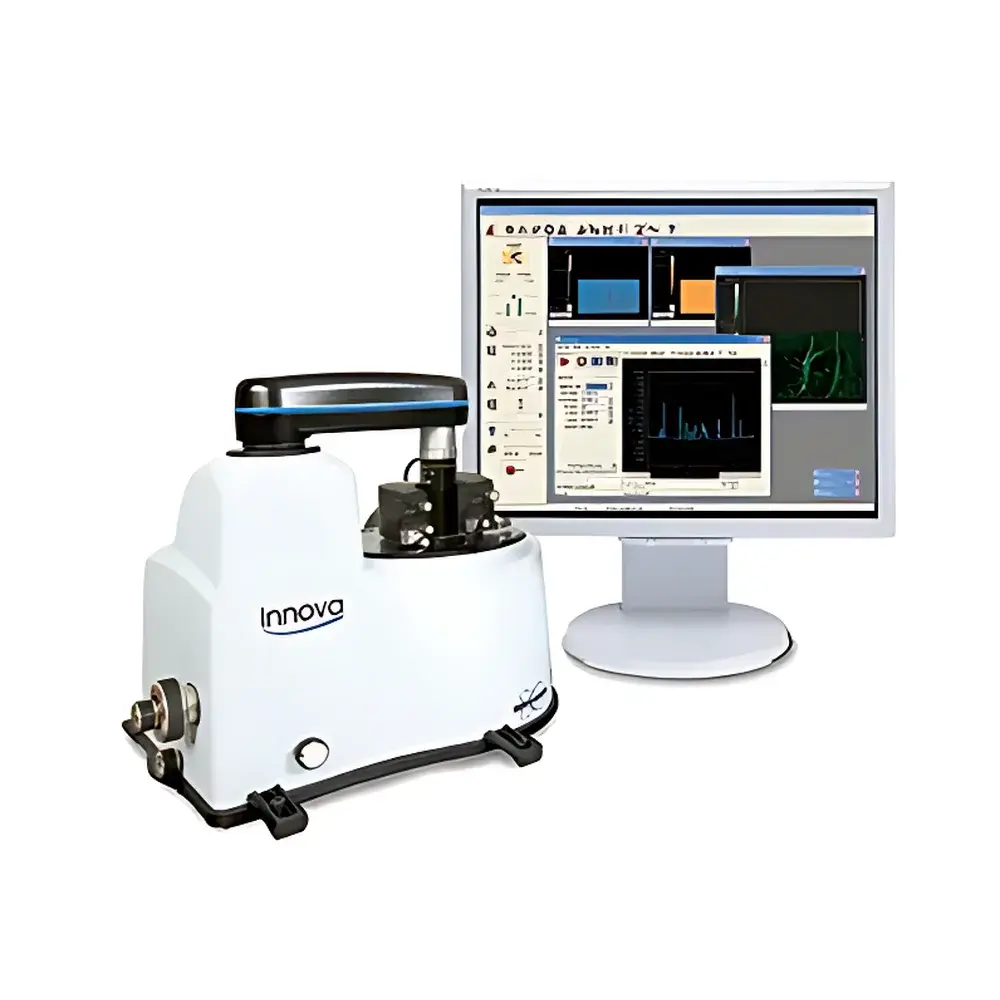
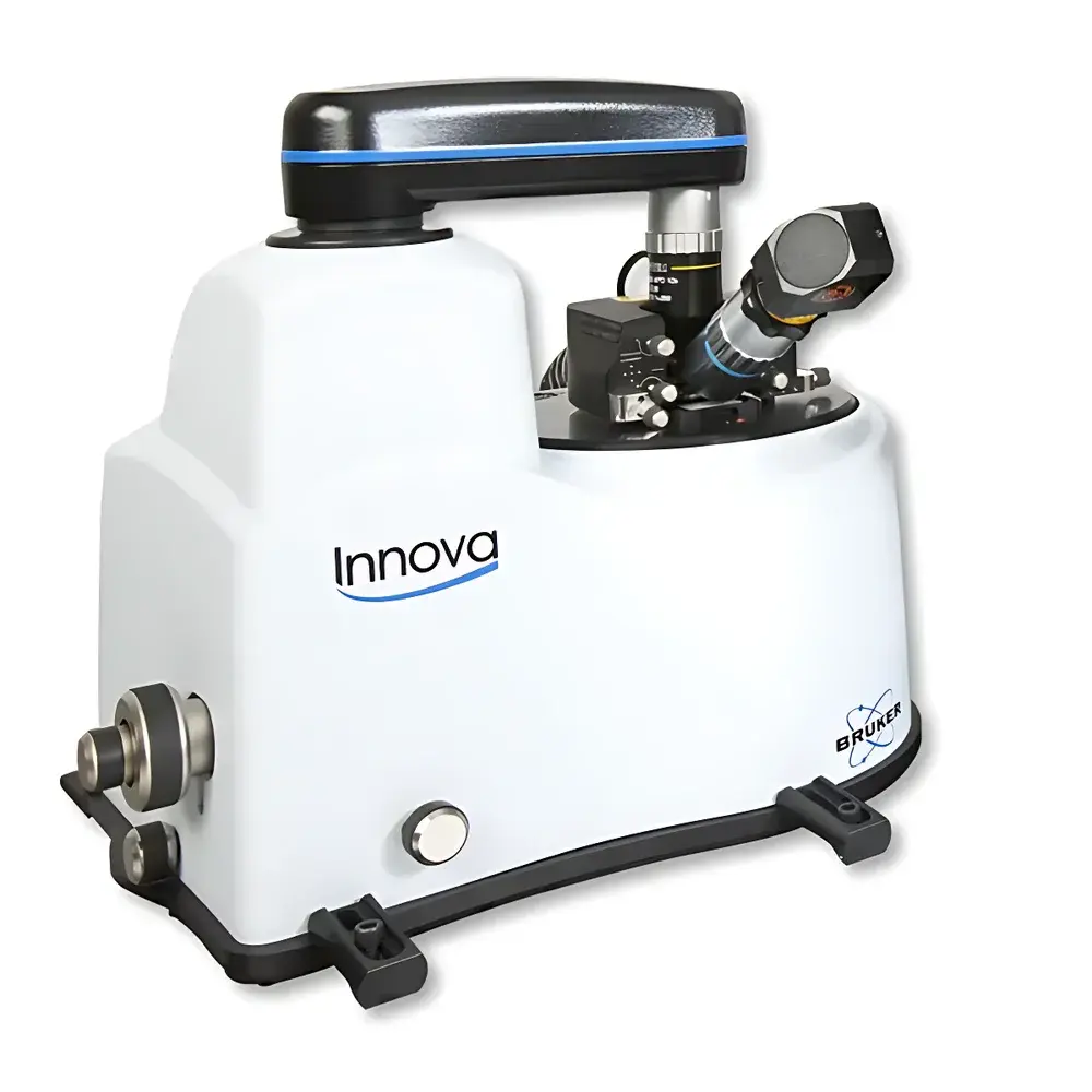
| Model | Innova |
| Instrument Type | Atomic Force Microscope (AFM) |
| Sample Stage Travel Range | 90 µm |
| Positional Detection Noise | < 0.1 nm (RMS, Z-axis, typical in air) |
| Maximum Sample Size Compatibility | 90 mm diameter × 25 mm height |
| Closed-Loop Scan Linearity | ±0.05% over full range |
| Z-Range | 10 µm (standard), upgradable to 15 µm |
| Optical Navigation Resolution | 1.3 MP color CCD with 4×–40× motorized zoom |
| AFM Mode Support | Contact, Tapping, Phase Imaging, Force Modulation, Lateral Force, Conductive AFM, Kelvin Probe Force Microscopy (KPFM), Magnetic Force Microscopy (MFM) |
| Brand | Bruker |
|---|---|
| Origin | USA |
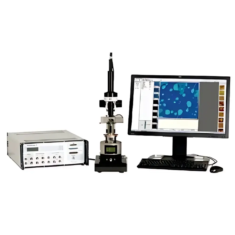
| Model | Innova |
| Instrument Type | Atomic Force Microscope (AFM) |
| Positioning Detection Noise | <2 µm (with standard 10× objective) |
| Sample Dimensions | 50 mm × 50 mm × 18 mm (X × Y × Z) |
| Z-Axis Stage Travel | 18 mm |
| Closed-Loop Scanner Range | XY > 90 µm, Z > 7.5 µm |
| Open-Loop Scanner Range | XY > 5 µm, Z > 1.5 µm |
| Optical Field of View | 1.24 mm × 0.25 mm (motorized zoom, 10× objective) |
| Optical Resolution | <2 µm (10×), <0.75 µm (50×) |
| Controller | 20-bit DAC, 100 kHz ±10 V ADCs |
| Software | SPMLab™ v7.0 (Windows® XP) |
| Brand | Bruker |
|---|---|
| Origin | USA |
| Model | MultiMode 8 |
| Instrument Type | Atomic Force Microscope (AFM) |
| Z-Direction Positioning Noise | <0.3 Å RMS (Tapping Mode, 0 nm scan size, with active vibration isolation) |
| Maximum Sample Size | 15 mm × 15 mm × 5 mm |
| XY Stage Travel Range | 15 mm × 15 mm |
| Optional Scan Heads | AS-0.5 (0.4 µm × 0.4 µm XY / 0.4 µm Z), AS-12 (10 µm × 10 µm XY / 2.5 µm Z), AS-130 (125 µm × 125 µm XY / 5.0 µm Z), PF50 (40 µm × 40 µm XY / 20 µm Z) |