
Scanning Probe Microscopes
Filter
Showing 31–60 of 110 results
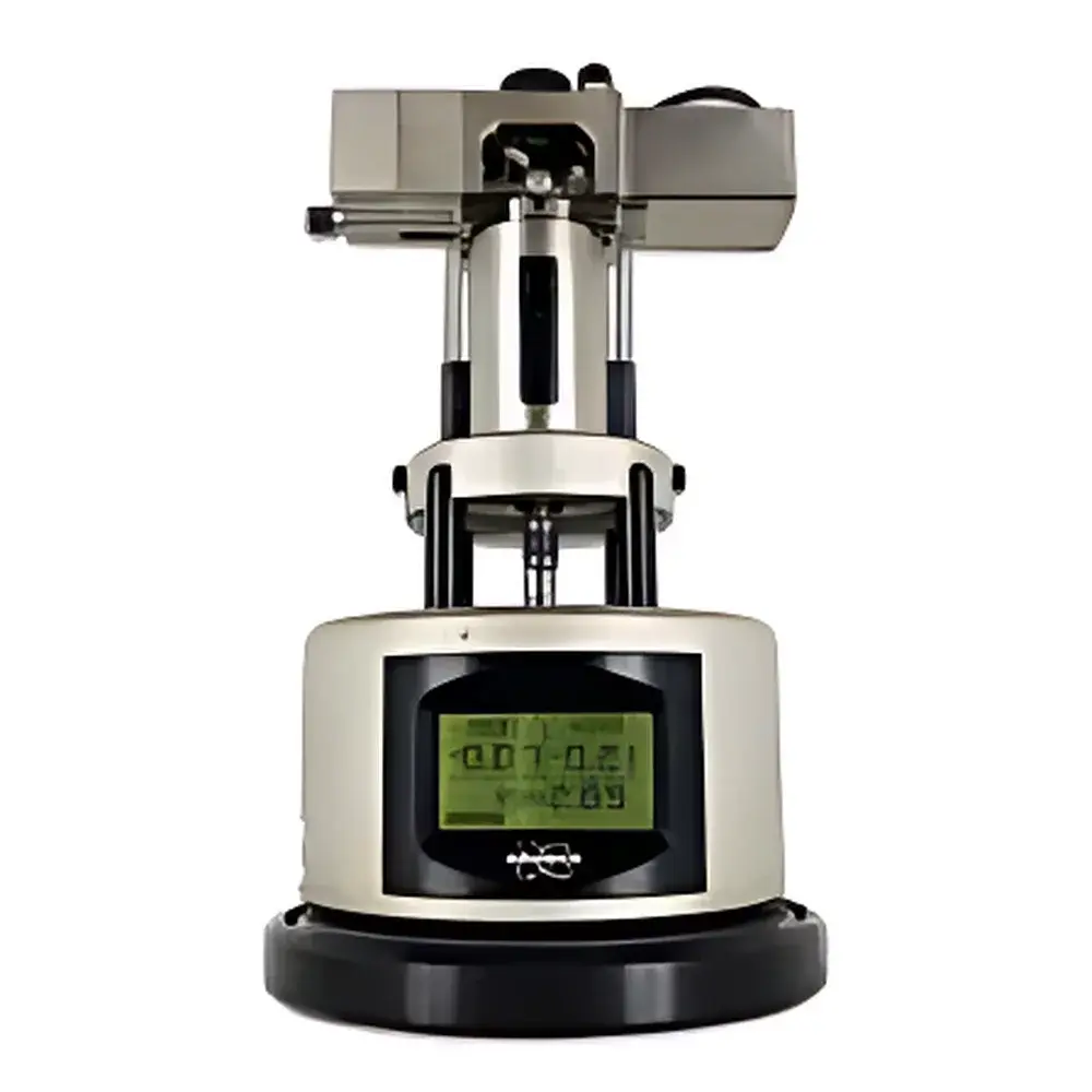
| Brand | Bruker |
|---|---|
| Origin | Germany |
| Model | MultiMode 8 |
| Instrument Type | Materials-Focused AFM |
| XY Positioning Noise | ≤0.15 nm |
| Maximum Sample Diameter | ≤15 mm |
| Maximum Sample Thickness | ≤5 mm |
| Sample Stage Travel Range | 180 mm × 180 mm (visible area) |
| Controller | NanoScope® V |
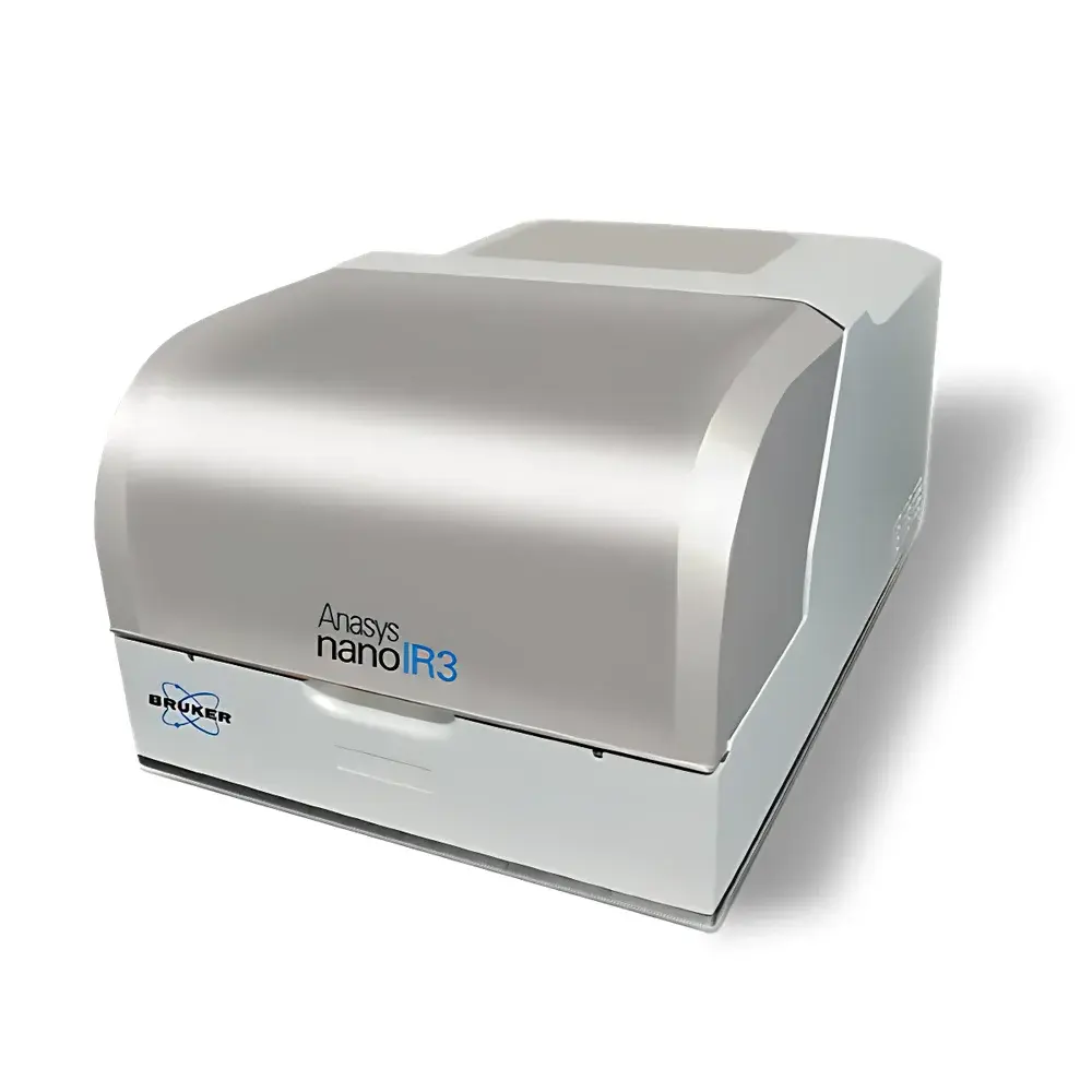
| Brand | Bruker |
|---|---|
| Origin | USA |
| Model | nanoIR3 |
| Instrument Type | Nano-Fourier Transform Infrared Spectrometer |
| Category | Scanning Probe Microscope–Integrated Optical Spectroscopy System |
| Compliance | ASTM E2947-21 (Standard Guide for Nanoscale Infrared Spectroscopy), ISO/IEC 17025–Accredited Measurement Capability Context |
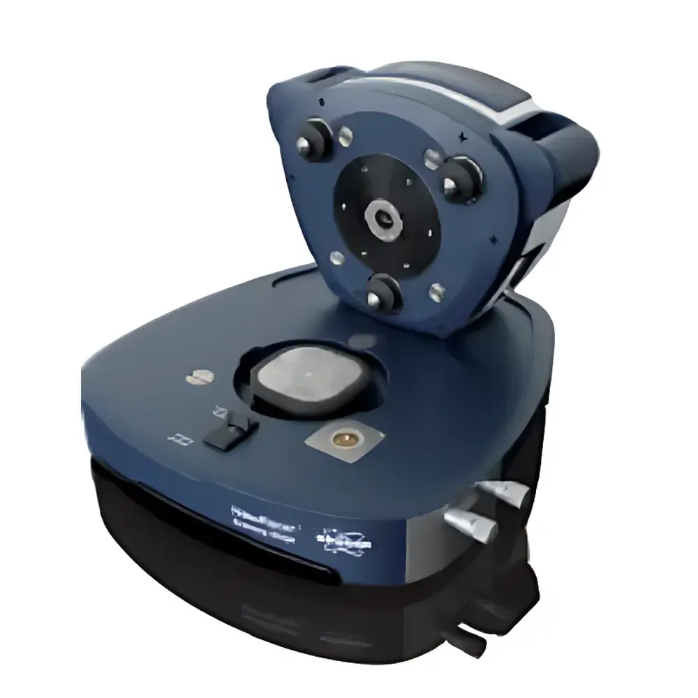
| Brand | Bruker |
|---|---|
| Origin | Germany |
| Manufacturer Type | Authorized Distributor |
| Origin Category | Imported |
| Model | NanoRacer |
| Instrument Type | Biological Atomic Force Microscope |
| XY Position Detection Noise | <0.09 nm RMS |
| Z Position Detection Noise | <0.04 nm RMS |
| Typical Sample Diameter | 4 mm |
| Software Version | V7 |
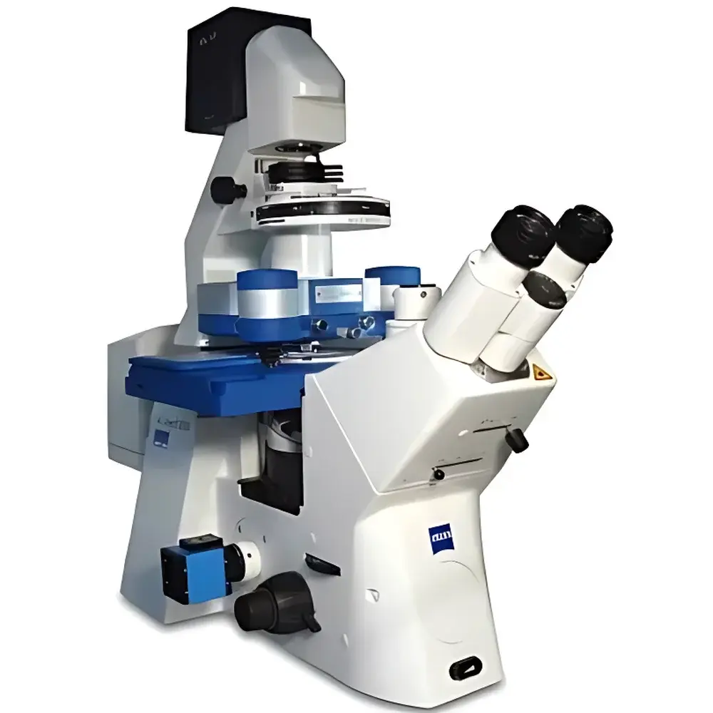
| Brand | Bruker |
|---|---|
| Origin | Germany |
| Model | NanoWizard 4 XP |
| Instrument Type | Biological Atomic Force Microscope |
| Position Detection Noise | X-Y direction RMS < 0.09 nm, Z direction RMS < 0.04 nm |
| Sample Scan Area | 100 µm × 100 µm × 15 µm |
| Stage Travel Range | 20 × 20 mm² |
| Software | V7 |
| Controller | Vortis™ 2 |
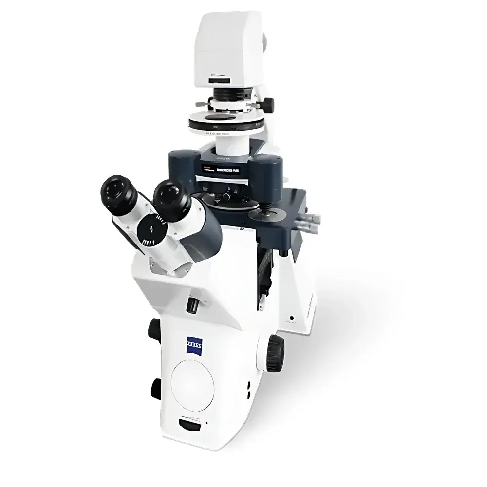
| Brand | Bruker |
|---|---|
| Origin | Germany |
| Model | NanoWizard PURE |
| Instrument Type | Biological Atomic Force Microscope |
| Category | Scanning Probe Microscope (SPM) |
| Architecture | Modular, Optically Compatible SPM Platform |
| Key Capabilities | Correlative Optical-AFM Imaging, Quantitative Nanomechanics, Multi-Modal Functional Imaging (PFM, MFM, EFM, KPFM, C-AFM, SSRM, STS, sThermal-AFM), Nanomanipulation & Nanolithography |
| Software Suite | JPK Instruments (now part of Bruker) SPMLab+, ExperimentalPlanner, RampDesigner, DirectOverlay2, DirectTiling |
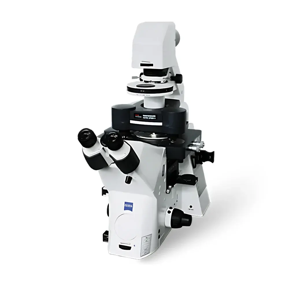
| Brand | Bruker |
|---|---|
| Origin | Germany |
| Model | ULTRA Speed 3 |
| Instrument Type | Biological Atomic Force Microscope |
| Category | Scanning Probe Microscope (SPM) |
| Architecture | Modular, Multi-Functional SPM Platform |
| Compliance | Designed for GLP/GMP-relevant environments with audit-trail-capable software |
| Data Format | Native HDF5 storage with metadata embedding |
| Automation Level | Fully integrated hardware-software automation for unattended operation |
| Software Framework | JPK Instruments’ BioAFM Suite (licensed and co-developed with Bruker) |
| Microscope Integration | Compatible with inverted optical microscopes (e.g., Zeiss Axio Observer, Nikon Ti2, Olympus IX83) |
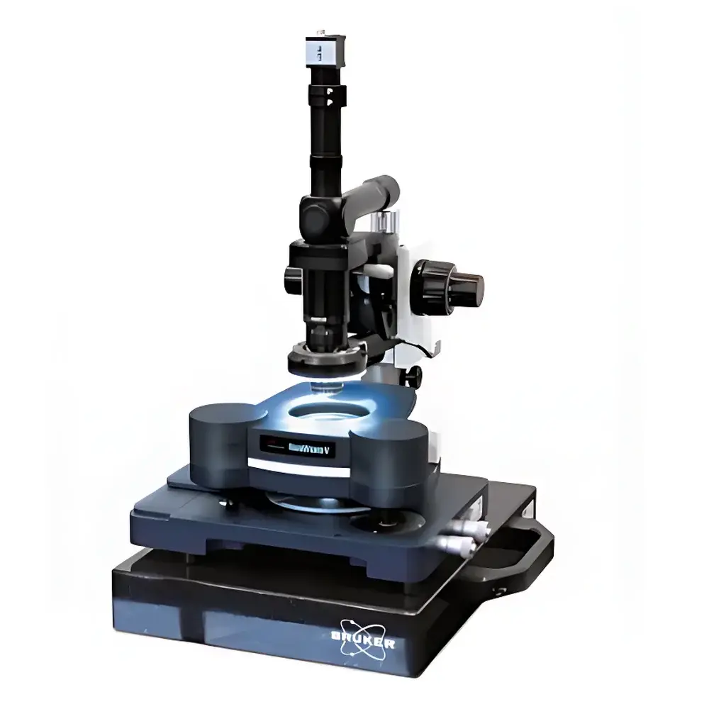
| Brand | Bruker |
|---|---|
| Origin | Germany |
| Model | NanoWizard V |
| Instrument Type | Biological Atomic Force Microscope |
| Sample Stage Travel Range | 20 × 20 mm² |
| Maximum Sample Height (with Head-Up Stage) | 140 mm Ø × 18 mm thickness |
| Free Sample Space | Ø140 × 18 mm³ |
| Software | V8 |
| Key Capabilities | PeakForce-QI, PeakForce Tapping®, PeakForce QNM®, Quantitative Imaging (QI), Single-Molecule Force Spectroscopy, Single-Cell Force Spectroscopy, DirectOverlay 2 for AFM–Optical Correlative Imaging, ExperimentPlanner & ExperimentControl modules, Integrated High-NA Optical Microscopy, Multi-Dimensional Environmental Control |
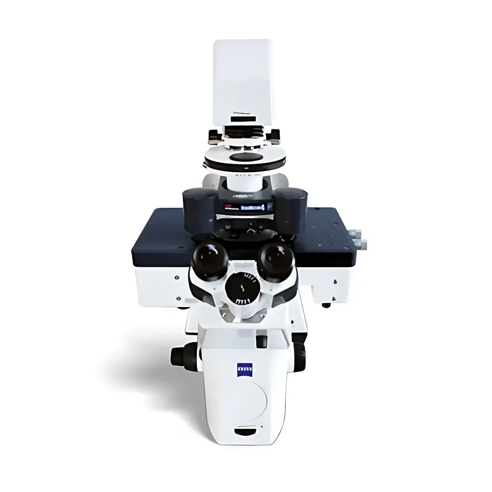
| Brand | Bruker |
|---|---|
| Origin | Germany |
| Model | NanoWizard® 4 XP BioScience |
| Instrument Type | Biological Atomic Force Microscope |
| Software Platform | V7 |
| Category | Scanning Probe Microscope |
| Import Status | Imported |
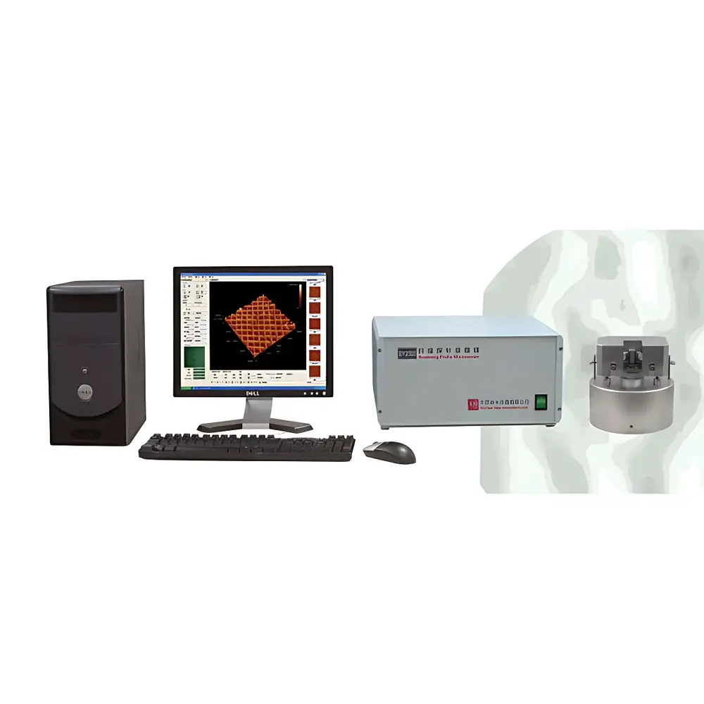
| Key | Brand: Benyuan Nanotechnology |
|---|---|
| Model | BY2000 |
| Origin | Beijing, China |
| Instrument Type | Atomic Force Microscope (AFM) / Scanning Tunneling Microscope (STM) / Lateral Force Microscope (LFM) |
| Vertical Position Detection Noise | 0.1 nm |
| Maximum Sample Diameter | 45 mm |
| Maximum Sample Thickness | 15 mm |
| XY Sample Stage Travel Range | 100 mm × 100 mm |
| XY Scan Range | ~10 μm |
| Z Scan Range | ~2 μm |
| Image Resolution Options | 128×128, 256×256, 512×512, 1024×1024 pixels |
| Scan Angle | 0–360° |
| Scan Frequency | 0.1–100 Hz |
| Controller | TI 32-bit DSP with Real-Time OS |
| DAC/ADC | 16-bit high-speed |
| High-Voltage Driver | 5-channel APEX integrated HV op-amps |
| Interface | 10/100 Mbps Fast Ethernet |
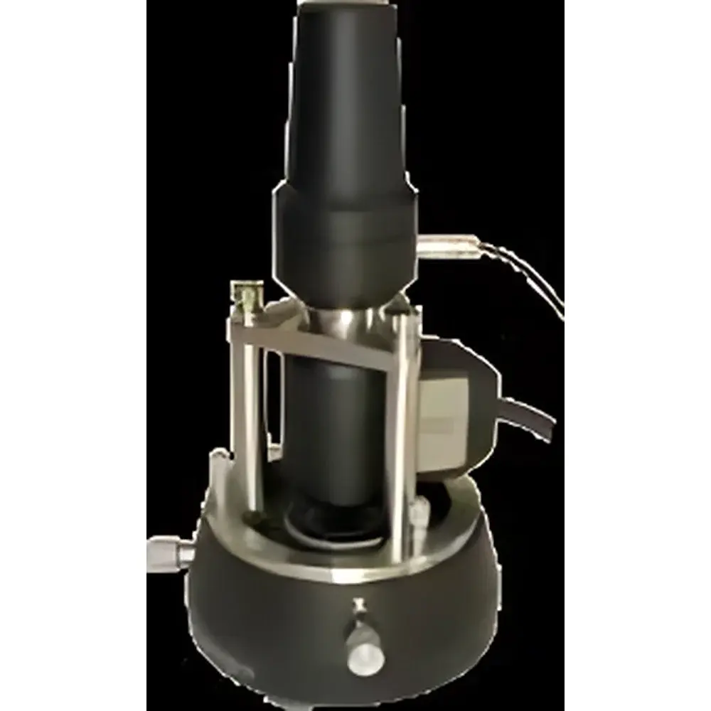
| Brand | DME |
|---|---|
| Origin | Denmark |
| Manufacturer Type | Authorized Distributor |
| Import Status | Imported |
| Model | DME DS 95 SPM |
| Price Range | USD 68,000 – 136,000 (est.) |
| Positional Noise | X-Y < 0.15 nm RMS, Z = 35 pm RMS |
| XY Stage Travel Range | 180 nm × 180 nm |
| Scan Volume Options | 50 × 50 × 5 µm (DS95-50) or 200 × 200 × 15 µm (DS95-200) |
| Max. Scan Rate | 30 Hz |
| Z-direction Mechanical Resolution (HOPG) | 0.06 nm RMS |
| Z-direction Electronic Noise Floor | < 0.05 nm RMS |
| Cantilever Insertion | Plug-and-Play |
| SPM Modes | AC Mode (Amplitude & Phase Imaging), LFM, MFM, KPFM, EFM, SCM, STM |
| Integrated Optical Axis | Yes |
| CCD-Based Visual Navigation | Yes |
| Controller Software | DiProWa, C26ScanTool (optional) |
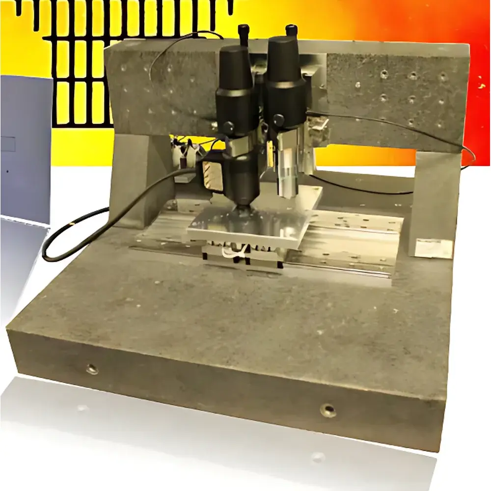
| Brand | DME |
|---|---|
| Origin | Denmark |
| Model | DS95Navi |
| Positioning Detection Noise | X-Y < 0.15 nm RMS, Z = 35 pm |
| Sample Dimensions | Diameter < 15 mm, Thickness < 5 mm |
| Sample Stage Travel Range | 180 nm × 180 nm |
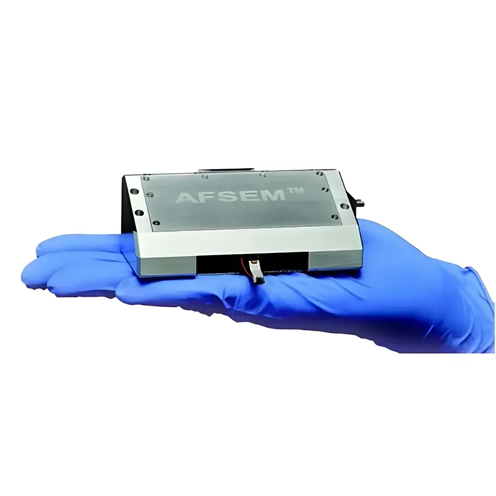
| Brand | GETec Microscopy |
|---|---|
| Origin | Austria |
| Model | AFSEM |
| Instrument Type | In-Situ AFM Integration System for SEM |
| Sample Dimensions | H = 41 mm, L = 110 mm, W = 77 mm |
| Stage Travel Range | X = ±4 mm (±7.5 mm optional), Y = ±4 mm, Z = 25 mm |
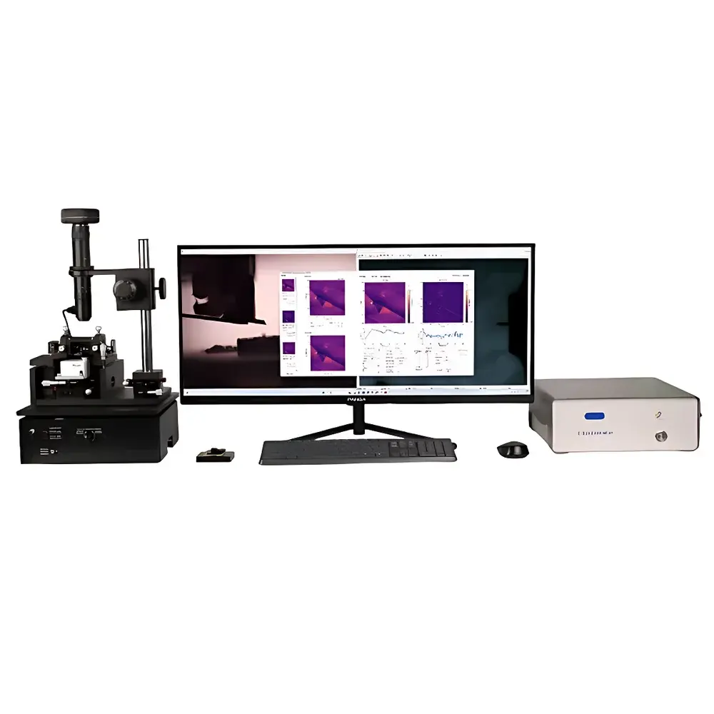
| Brand | Grapes |
|---|---|
| Origin | Zhejiang, China |
| Manufacturer Type | Direct Manufacturer |
| Instrument Type | Atomic Force Microscope (AFM) |
| Model | HR-AFM |
| Price Range | USD 69,500 – 139,000 |
| XY Positioning Noise | ≤0.2 nm RMS |
| Z Positioning Noise | ≤30 pm RMS |
| Sample Diameter | ≤25.4 mm |
| Sample Thickness | ≤6.35 mm |
| Sample Stage Travel Range | 25.5 mm × 25.5 mm × 18 mm |
| Z-Axis Resolution | ≤0.03 nm RMS |
| Optical Top View Camera | ≥3 MP CMOS, Optical Resolution ≤2 µm, FOV Adjustable from 2 mm × 2 mm to 300 µm × 300 µm, Magnification 45×–400× (Mechanically Adjustable) |
| Side View Camera | Real-time cantilever approach monitoring for precise tip engagement and collision avoidance |
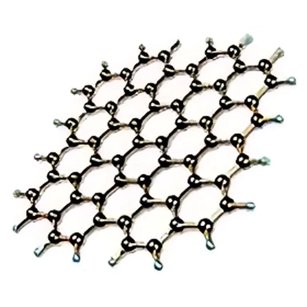
| Origin | USA |
|---|---|
| Supplier Type | Authorized Distributor |
| Import Status | Imported |
| Available Volumes | 50 mL, 100 mL, 200 mL, 500 mL (aqueous or organic dispersion) |
| Pricing | Upon Request |
| Brand | Hitachi |
|---|---|
| Origin | Japan |
| Manufacturer | Hitachi High-Tech Corporation |
| Type | Atomic Force Microscope (AFM) |
| Model | AFM100 |
| Instrument Category | Materials-Grade AFM |
| Position Detection Noise | 0.03 nm |
| Maximum Sample Diameter | ≤35 mm |
| Maximum Sample Thickness | ≤10 mm |
| Sample Stage Travel Range | 5 mm |
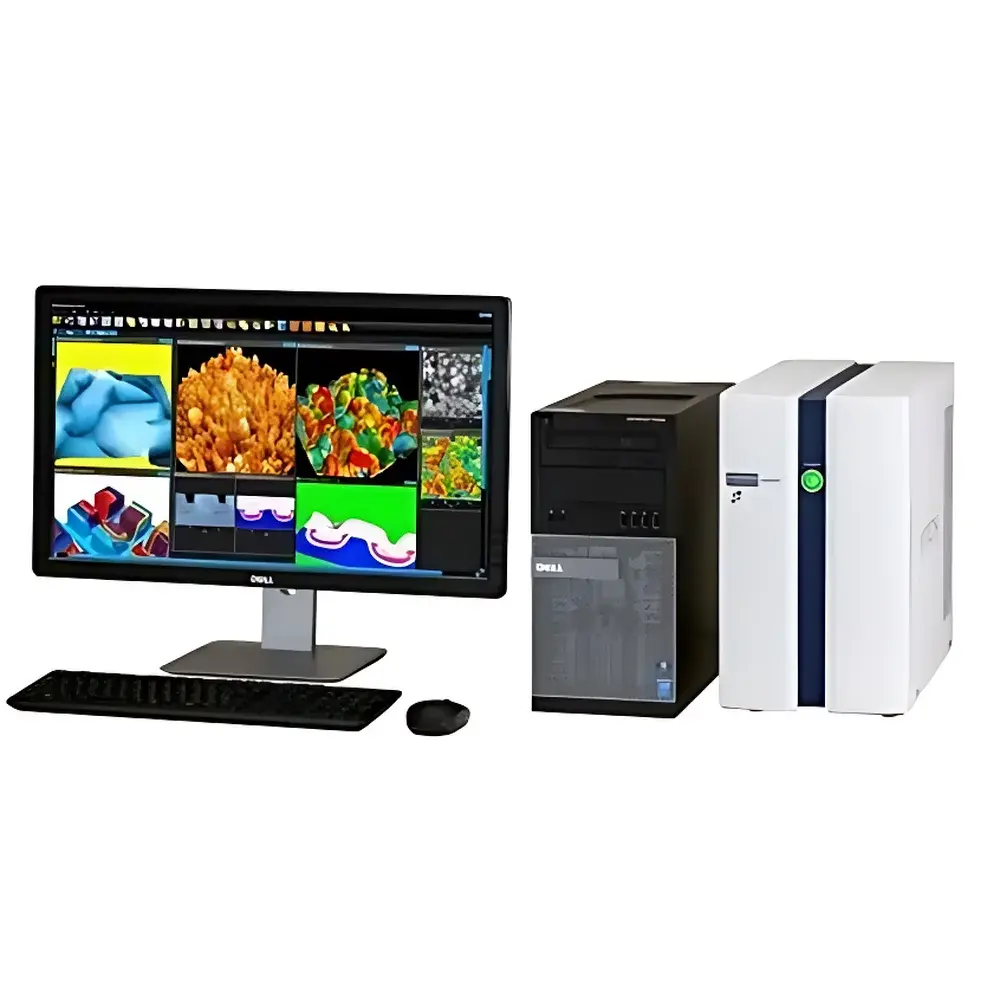
| Brand | Hitachi |
|---|---|
| Origin | Japan |
| Manufacturer | Hitachi High-Tech Science Corporation |
| Product Type | Atomic Force Microscope (AFM) Controller |
| Model | AFM5000II / RealTune®II |
| Compliance | Designed for ISO/IEC 17025-compliant labs |
| Software Architecture | Windows-based real-time control platform with audit trail capability |
| Control Resolution | Sub-nanometer positioning accuracy |
| Vibration Noise Floor | < 0.1 nm RMS (in closed-loop mode) |
| Sample Stage Travel Range | X/Y: ±25 µm, Z: ±5 µm |
| GUI Framework | Qt-based modular interface with tabbed workflow navigation |
| 3D Rendering Engine | OpenGL-accelerated volumetric reconstruction |
| Data Format | HDF5-compliant binary + metadata-rich XML header |
| Regulatory Alignment | Supports FDA 21 CFR Part 11 electronic signature and ALCOA+ data integrity principles |
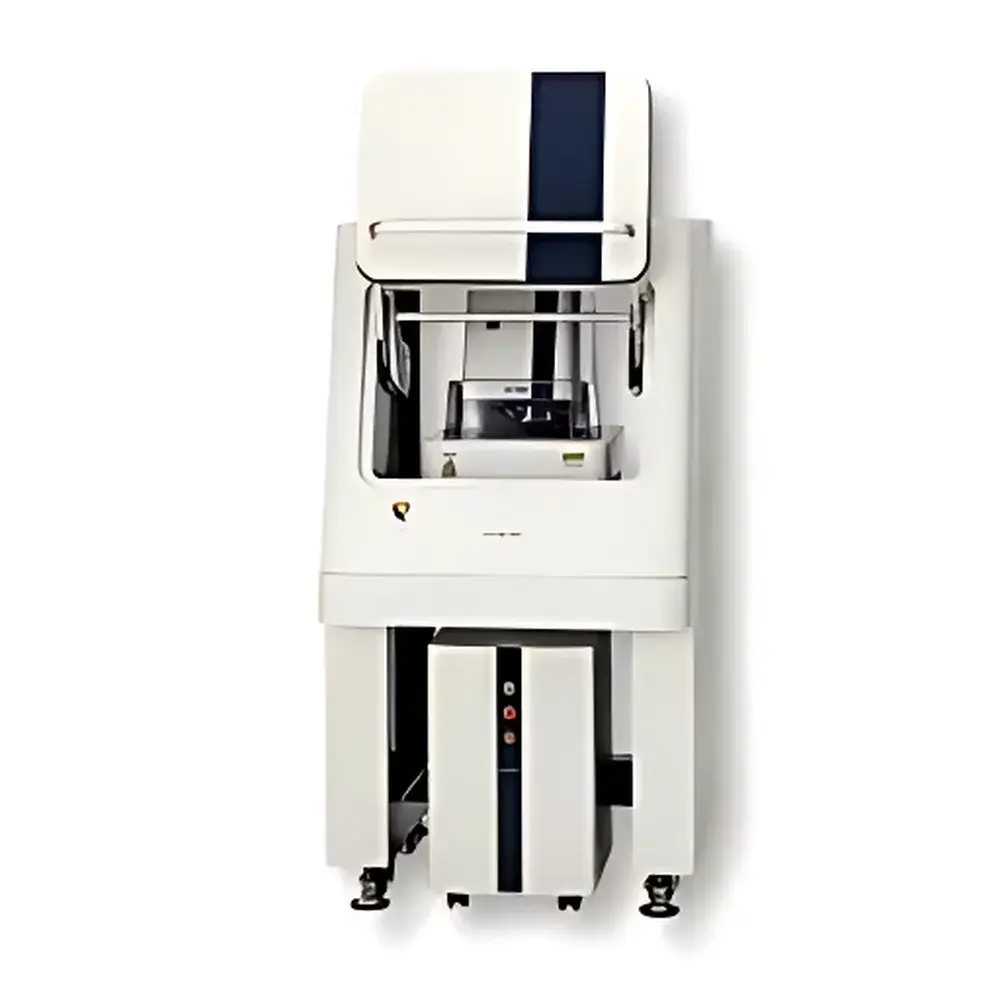
| Brand | Hitachi |
|---|---|
| Origin | Japan |
| Manufacturer Type | Original Equipment Manufacturer (OEM) |
| Product Category | Imported Instrument |
| Model | AFM5500M II |
| Instrument Type | Atomic Force Microscope (AFM) |
| Application Class | Materials Science AFM |
| Position Detection Noise | ≤ 0.04 nm (High-Resolution Mode) |
| Sample Diameter | ≤ 100 mm |
| Sample Thickness | ≤ 20 mm |
| XY Stage Travel Range | 100 mm × 100 mm |
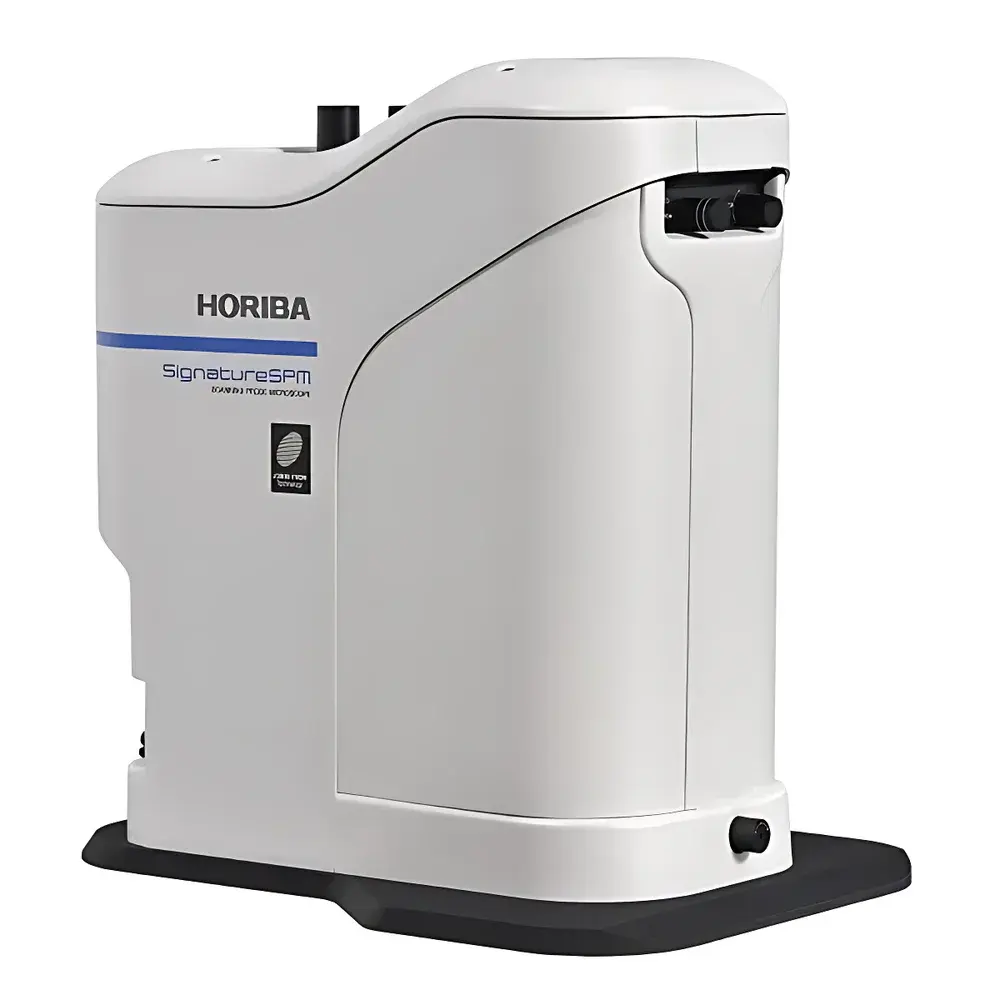
| Brand | HORIBA |
|---|---|
| Origin | France |
| Manufacturer Type | Manufacturer |
| Import Status | Imported |
| Model | Signature SPM |
| Instrument Category | Atomic Force Microscope |
| Instrument Type | Materials-Focused AFM |
| Spectroscopy Integration | Confocal Raman & Photoluminescence (PL) |
| Core Capability | True Co-Localized Multimodal Imaging (Topography + Nanomechanics + Electrostatics + Magnetism + Chemical Fingerprinting) |
| Scanner Range | 100 × 100 × 15 µm |
| Optical Access | Dual-Path, IR AFM Laser (1310 nm) + Visible/NIR Excitation Lasers (e.g., 532 nm, 638 nm, 785 nm) |
| Spectrometer | Achromatic, >95% Reflectivity, Triple-Grating Support (150–6000 cm⁻¹) |
| Software Feature | “Probe Away” / “Probe Back” Automated Tip Retraction & Re-Registration |
| Compliance | Designed for GLP/GMP-adjacent research environments |
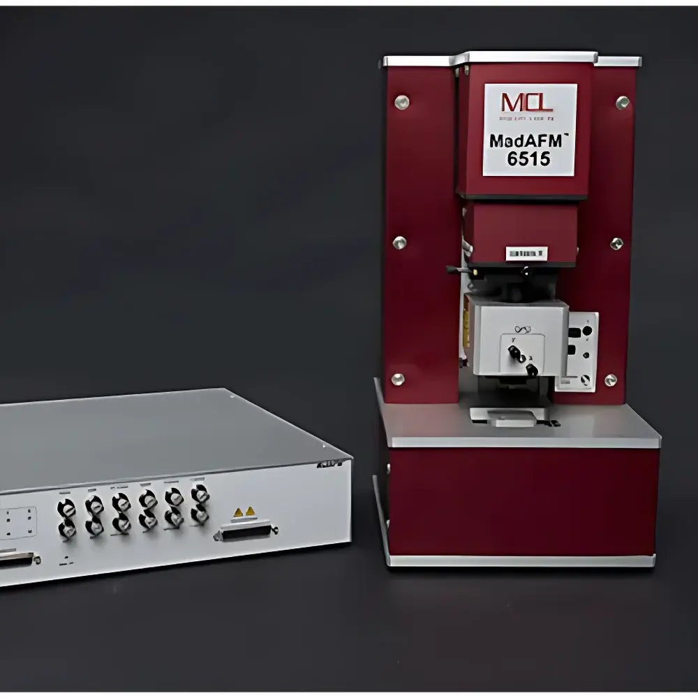
| Brand | MCL Think Nano |
|---|---|
| Origin | USA |
| Model | MadAFM™ |
| Instrument Type | Material-Grade AFM |
| Positional Detection Noise | <0.15 nm RMS |
| Max Sample Size | 50 mm × 50 mm × 40 mm |
| XY Sample Stage Travel | 25 mm |
| Z Focus & Head Travel | 50 mm |
| Closed-Loop Nanopositioner Range (XY) | 30/65/100 µm |
| Z Nanopositioner Range | 15/30 µm |
| Nanopositioner Resolution (30 µm range) | 0.03 nm |
| Nanopositioner Noise Floor (peak-to-peak) | 2.7 pm |
| Optical Alignment | 635 nm Class II laser + 1.6 MP coaxial CMOS camera |
| Software | AFMView®-OD (USB 2.0 interface, Windows 8.1/10/11) |
| Brand | MCL Think Nano |
|---|---|
| Origin | USA |
| Manufacturer Type | Authorized Distributor |
| Import Status | Imported |
| Model | MadPLL® |
| Price Range | USD $14,000 – $72,000 (based on configuration) |
| Positional Detection Noise | 0.15 nm RMS |
| Sample Diameter Limit | <15 mm |
| XY Scan Range (with compatible stages) | up to 200 µm |
| Z-Range (with Nano-OP30) | 30 µm (closed-loop), 100 µm (open-loop) |
| PLL Frequency Lock Range | 10–100 kHz |
| Phase Shift Resolution | <0.1° |
| Demodulation Bandwidth | 3 kHz |
| PCC Compensation Range | ±50 pF |
| Operating Systems | Windows 7/10/11 (32/64-bit), LabVIEW 2015+ compatible |
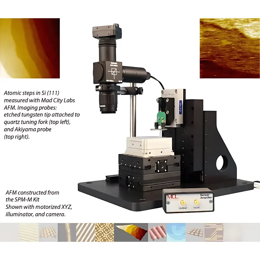
| Brand | MCL Think Nano |
|---|---|
| Origin | USA |
| Model | SPM-M Kit |
| Detection Noise | <0.15 nm RMS |
| Sample Size | <15 mm |
| XY Scan Range | 200 × 200 µm |
| Z Positioning | Nano-OP30 (closed-loop optional) |
| Controller | 3-Axis Nano-Drive® with PicoQ® sensors |
| Probe Options | Quartz tuning forks (5 included), Akiyama probe boards, tungsten tip etching compatibility |
| Software | AFMView™ with automated PLL control |
| Compliance | Designed for GLP/GMP-aligned research environments |
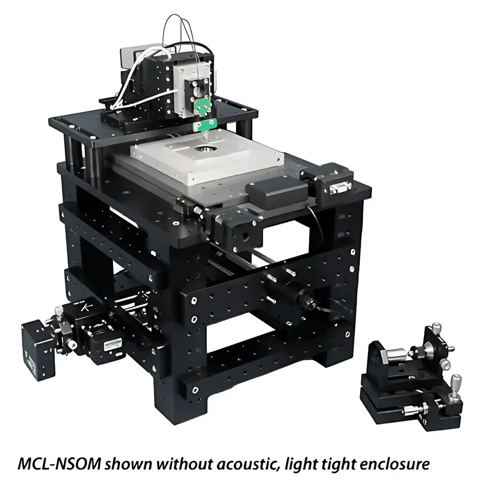
| Brand | MCL Think Nano |
|---|---|
| Origin | USA |
| Manufacturer Type | Authorized Distributor |
| Origin Category | Imported |
| Model | MCL-NSOM |
| Instrument Type | Materials-Focused NSOM System |
| Positioning Noise | X-Y ≤ 0.15 nm RMS, Z = 35 pm RMS |
| Typical Imaging Bandwidth | 625 Hz |
| Sample Dimensions | Ø ≤ 15 mm, Thickness ≤ 5 mm |
| Sample Stage Travel Range | Ø ≤ 15 mm, Thickness ≤ 5 mm |
| XY Micropositioner Range | 25 mm |
| Z Lens Micropositioner Range | 50 mm |
| Fiber XYZ Micropositioner Range | 25 mm |
| Micropositioner Step Size | 95 nm |
| Piezo Nanopositioner Range (XYZ) | 200 µm × 200 µm × 30 µm |
| Piezo Resolution | 0.4 nm (XY), 0.06 nm (Z) |
| Piezo Step Size | 0.2 nm (XY), 0.03 nm (Z) |
| Excitation Source | 635 nm, 5 mW laser diode with fiber coupling |
| Objective | 20× oil immersion, 0.4 NA, infinity-corrected |
| Detection | Avalanche photodiode (200–1000 nm, 1 mm active area) |
| Alignment Camera | 0.3 MP CMOS |
| Feedback Mode | Shear-force |
| NSOM Modes | Illumination, Collection, Illumination+Collection, Reflection, Reflection+Collection |
| Control Software | AFMView™ and LabVIEW™-based automation suite |
| Controller Interfaces | USB 2.0, 20-bit DAC/ADC, 4-channel TTL I/O |
| Operating System Compatibility | Windows Vista/7/8/10 |
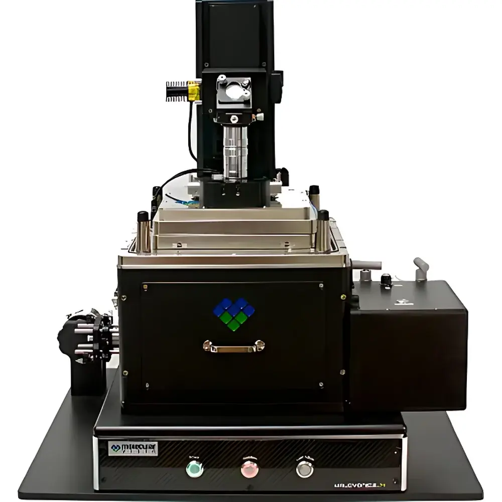
| Brand | Molecular Vista |
|---|---|
| Origin | USA |
| Model | Vista-SNOM |
| Positioning Detection Noise | ≤ 50 pm RMS |
| Sample Size | Ø ≤ 25 mm, Thickness ≤ 10 mm |
| Sample Stage Travel Range | 6 mm × 6 mm |
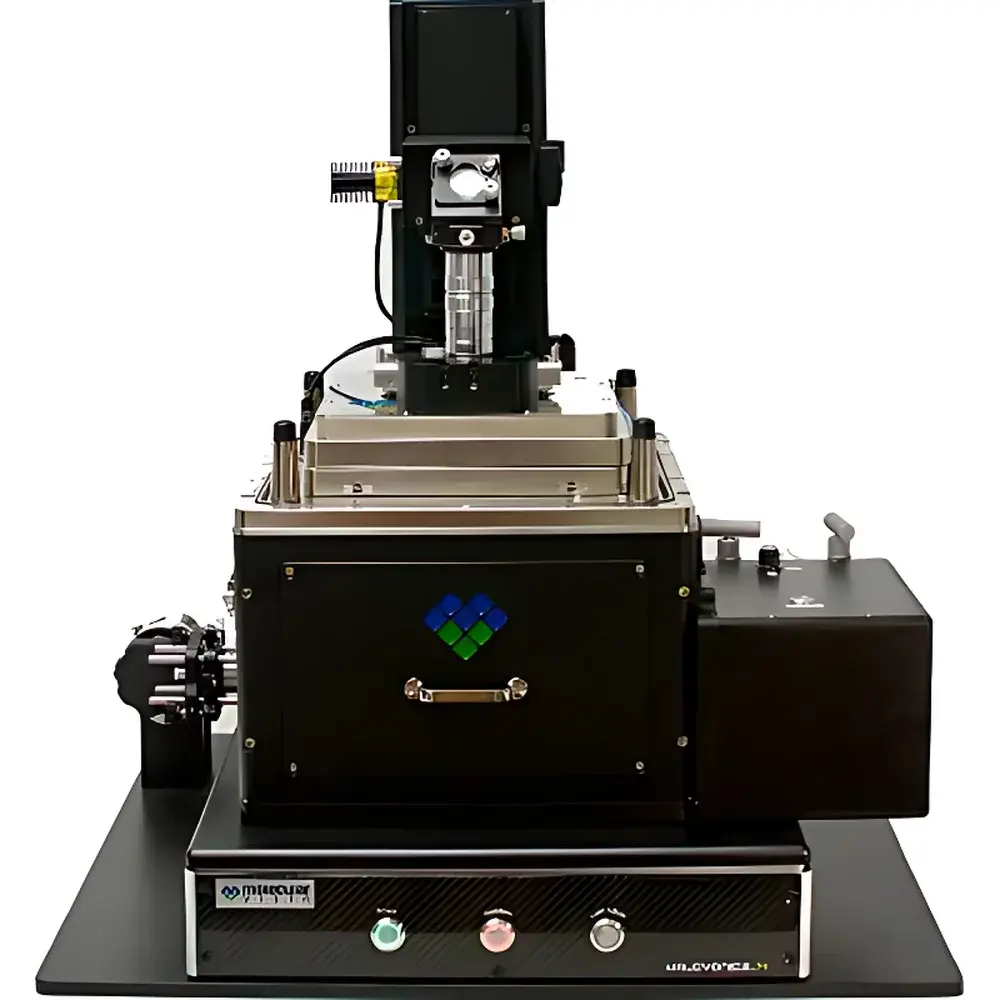
| Brand | Molecular Vista |
|---|---|
| Origin | USA |
| Manufacturer Type | Authorized Distributor |
| Origin Category | Imported |
| Model | VistaScope |
| Price Range | USD 420,000 – 700,000 |
| Instrument Type | Material Science AFM |
| Position Detection Noise | ≤ 50 pm RMS |
| Sample Dimensions | Ø ≤ 25 mm, Thickness ≤ 10 mm |
| XY Stage Travel Range | 6 mm × 6 mm |
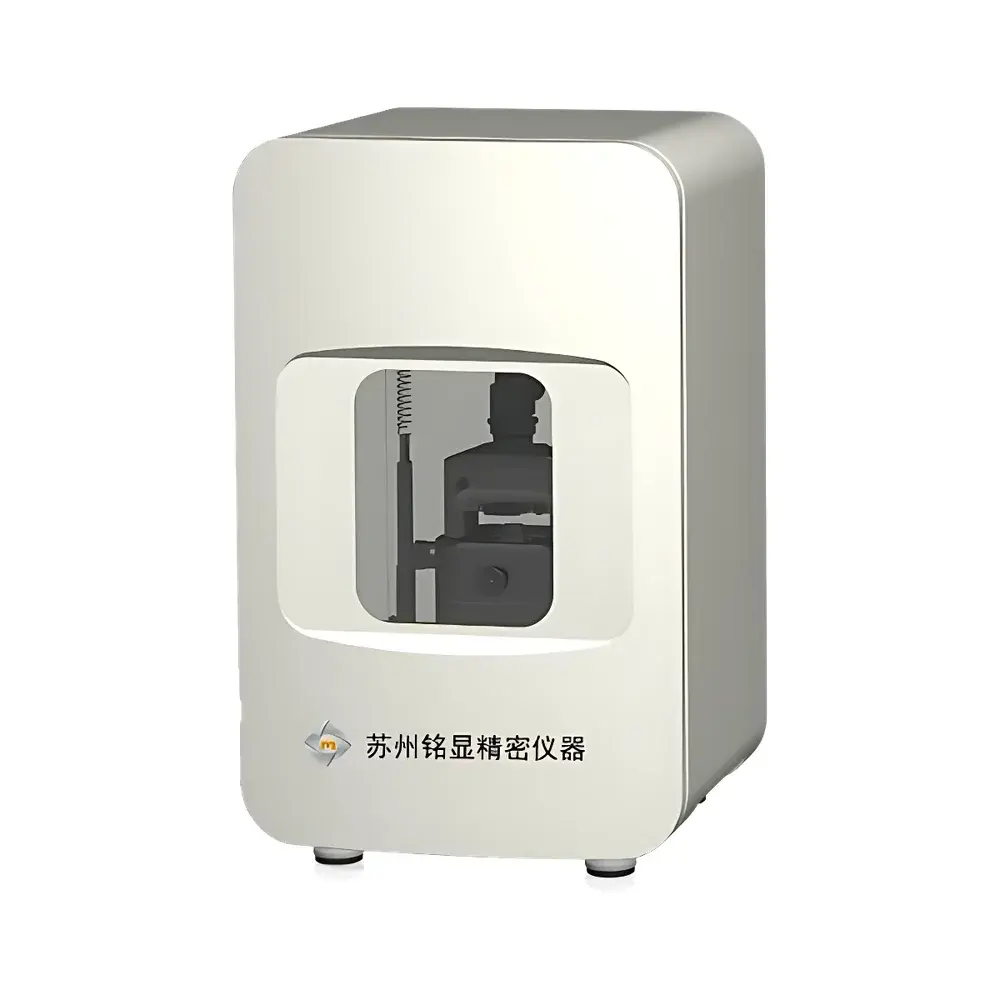
| Brand | MX-AFM |
|---|---|
| Origin | Jiangsu, China |
| Manufacturer Type | Authorized Distributor |
| Country of Origin | China |
| Model | MX-plorer Premium |
| Instrument Type | Atomic Force Microscope (AFM) |
| Position Detection Noise | ≤ 50 pm |
| XY Sample Stage Travel Range | ≥ 5 mm |
| Operating Modes | Contact, Tapping, Phase Imaging, Conductive AFM (C-AFM), Kelvin Probe Force Microscopy (KPFM), Force Spectroscopy, Nanolithography |
| Control Architecture | Closed-Loop Piezoelectric Scanning System |
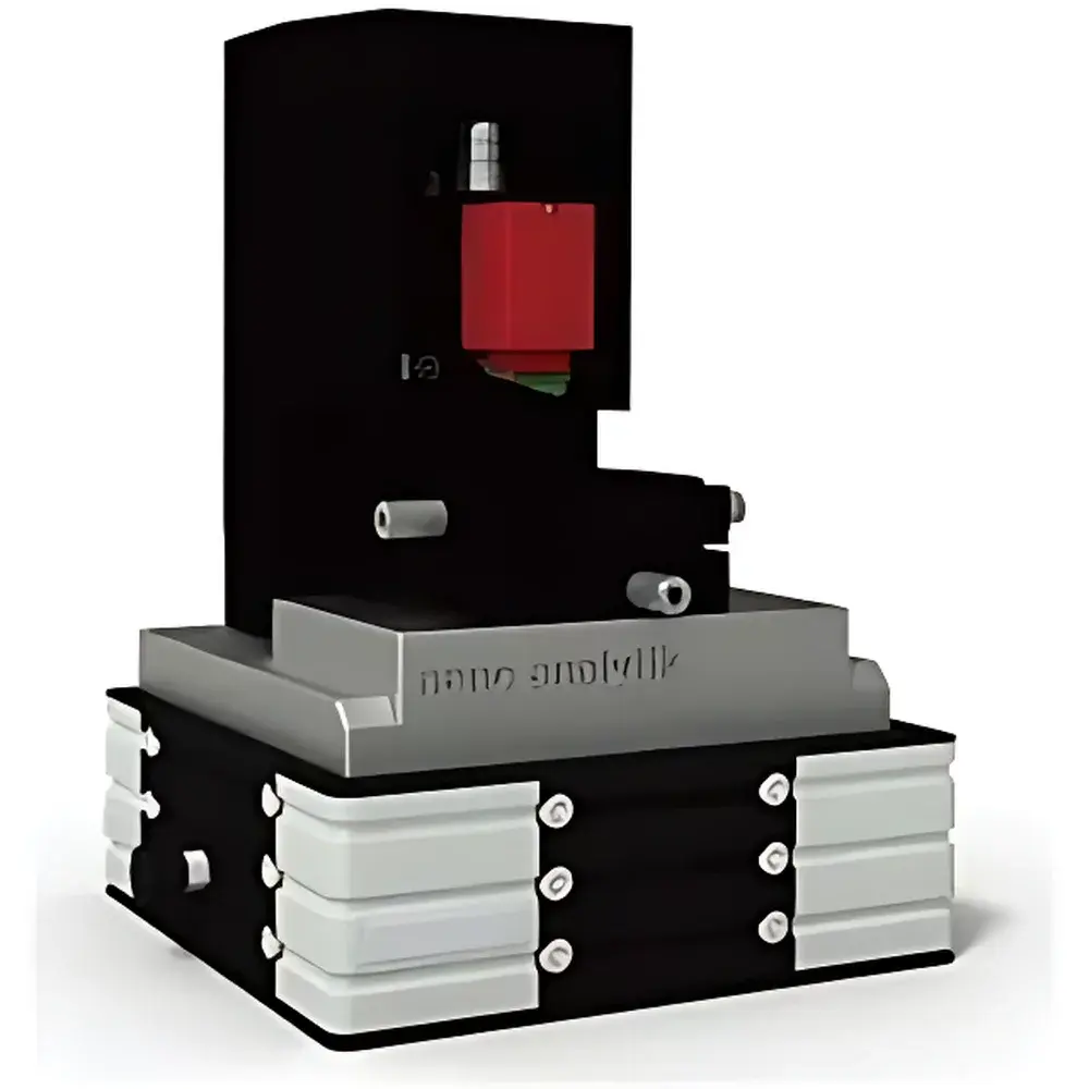
| Brand | Nano analytik |
|---|---|
| Origin | Germany |
| Model | AFM Series (SmartProbe Platform) |
| Instrument Type | Atomic Force Microscope |
| Vertical Position Detection Noise | 0.01 nm RMS |
| Maximum Sample Diameter | ≤10 cm |
| Scanner Range (Adeona) | 15 µm × 15 µm × 4 µm |
| Dimensions (Vacuum-Compatible Version) | 140 mm × 100 mm × 60 mm |
| Integrated Actuation & Sensing | Piezoresistive readout + bimaterial excitation on SmartProbe |
| XYZ Nanopositioning Range (Vacuum Variant) | 20 µm × 10 µm × 10 µm |
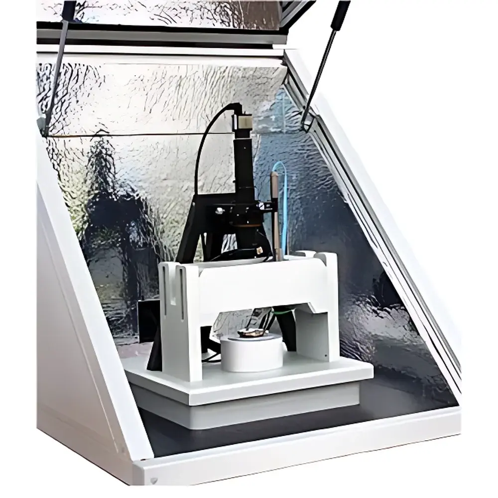
| Brand | Nano analytik |
|---|---|
| Origin | Germany |
| Model | SPL |
| Instrument Type | Atomic Force Microscope-based Scanning Probe Lithography System |
| Positioning Detection Noise | 0.01 nm (X, Y, Z) |
| Maximum Sample Diameter | 150 mm (6 in) |
| Stage Travel Range | 18 mm × 18 mm (expandable to 150 mm × 150 mm) |
| Minimum Feature Size | 5 nm (verified) |
| Direct-Write Speed | 300 µm/s |
| Overlay Accuracy | < 7 nm |
| Stitching Accuracy | < 10 nm |
| Maximum Writing Area per Field | 200 µm × 200 µm |
| Footprint | 80 cm × 100 cm × 190 cm |
| AFM Imaging Range | 10 µm × 10 µm × 5 µm (expandable to 200 µm × 200 µm) |
| Vertical RMS Noise | 0.01 nm |
| Closed-Loop Scan Linearity | 99.7% |
| Real-Time FPGA Feedback Bandwidth | 8 MHz |
| Data Acquisition Resolution | 16-bit (amplitude/phase) |
| Output Formats | BMP, PNG, JPG, TXT |
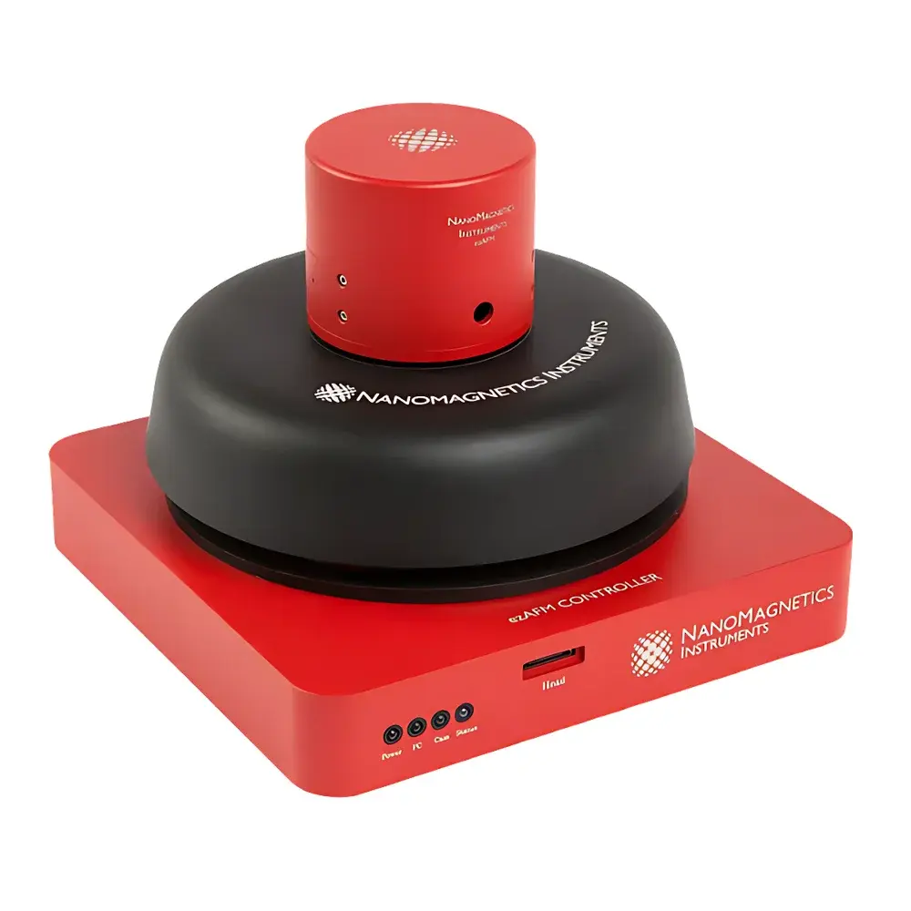
| Brand | NanoMagnetics |
|---|---|
| Origin | United Kingdom |
| Model | ezAFM |
| Instrument Type | Material-Grade AFM |
| Position Detection Noise | 75 fm/√Hz |
| Maximum Sample Dimensions | 10 × 10 × 5 mm |
| XY Stage Travel Range | 38 × 38 mm |
| Scan Areas | 120 × 120 × 40 µm (Z resolution: 0.2 nm) or 40 × 40 × 4 µm (Z resolution: 0.02 nm) |
| Lateral Resolution | 16 nm (large scan) / 5 nm (high-res scan) |
| Optical View System | Full HD CCD, 2 µm resolution, 390 × 230 µm FOV, 2516 × 1960 pixels, 30 fps |
| Controller | 24-bit ADC/DAC, FPGA/DSP-based digital feedback |
| Standard Imaging Modes | Contact, Tapping, Phase, LFM, MFM |
| Extended Modes (ezAFM+) | EFM, KPFM, C-AFM, SSRM, PRFM, FMM, nanomechanical mapping, liquid-phase, vacuum-compatible configurations |
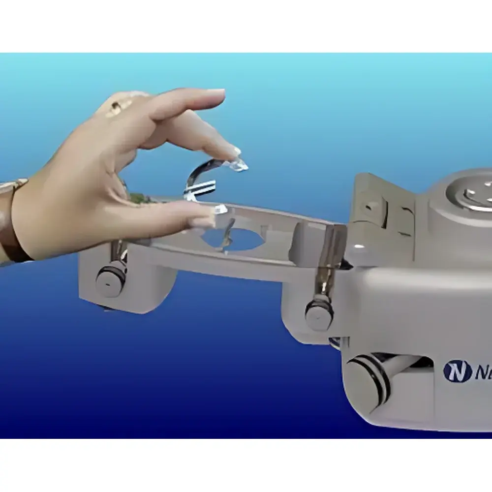
| Brand | Nanonics |
|---|---|
| Origin | Israel |
| Model | Academia |
| Instrument Type | Materials-Focused AFM |
| Primary Technique | Combined Scanning Probe Microscopy (SPM) with Integrated Near-Field Optical & Raman Capabilities |
| Scan Range | XY = 70 µm, Z = 5 µm (optional 10 µm scanner) |
| Positional Resolution | <1 nm (70 µm scanner), <0.1 nm (10 µm scanner) |
| Max Sample Size | 15 mm × 15 mm |
| Detection Method | Optical Beam Deflection |
| Operational Modes | Contact, Non-Contact, Tapping |
| Probe Compatibility | Nanonics glass probes, electro-thermal probes, NanoFountainPen™, and standard commercial SPM cantilevers |
| Software Platform | LabVIEW-based modular architecture with user-customizable modules |
| Compliance Ready | Designed for GLP/GMP-aligned workflows |
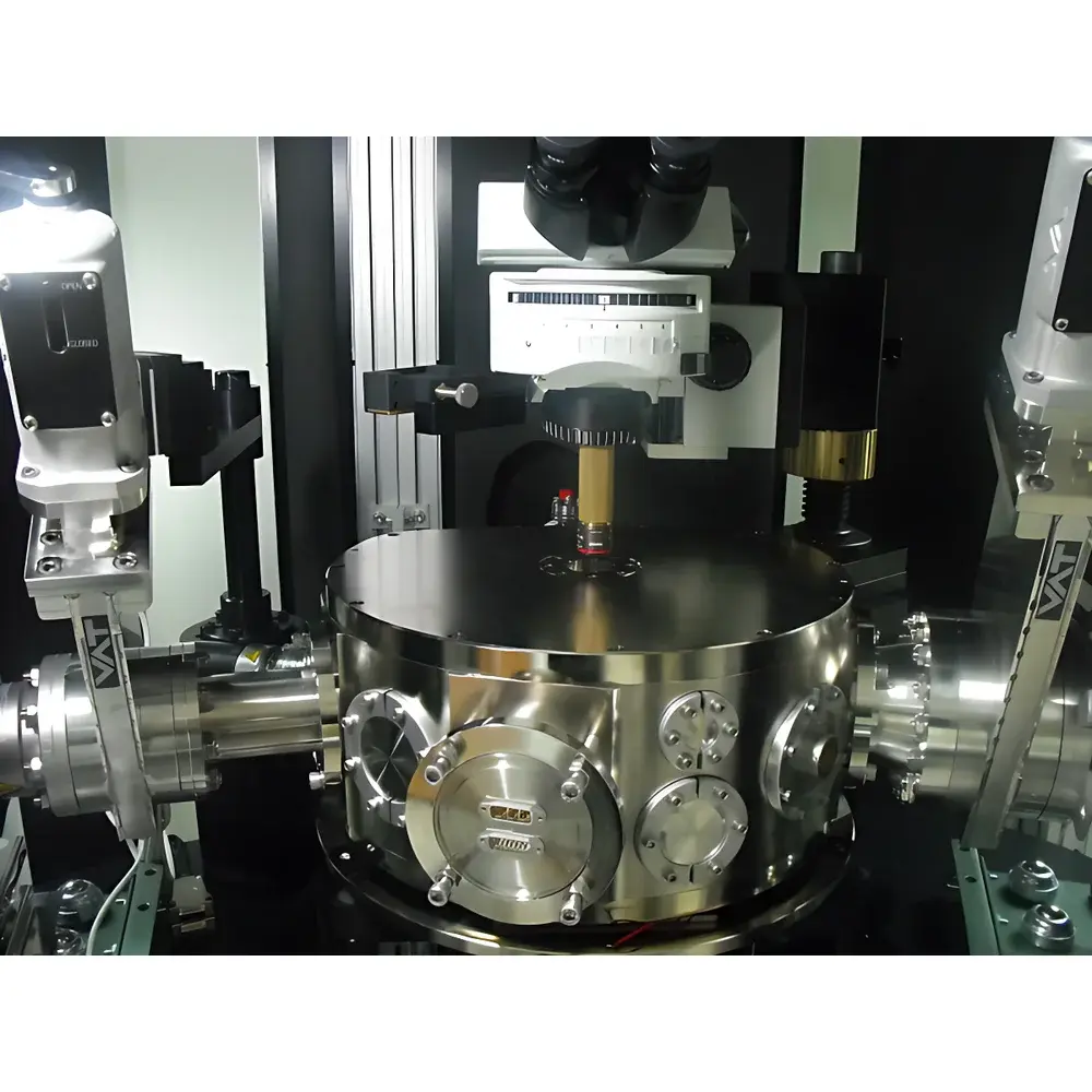
| Brand | Nanonics |
|---|---|
| Origin | Israel |
| Model | CryoView4000 |
| Z-positioning noise | <0.2 nm |
| Sample diameter | <100 mm |
| Sample thickness | <30 mm |
| Sample stage travel range | 80 µm × 80 µm × 70 µm |