
Scanning Probe Microscopes
Filter
Showing 91–110 of 110 results
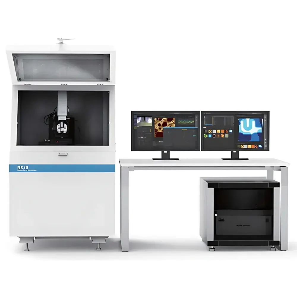
| Origin | South Korea |
|---|---|
| Manufacturer Type | Authorized Distributor |
| Origin Category | Imported |
| Model | NX20 |
| Price Range | USD 195,000 – 260,000 (FOB) |
| Instrument Type | Atomic Force Microscope |
| Application Class | Materials Science AFM |
| XY Positional Noise | < 0.25 nm (over 80 µm scan range) |
| Z-Noise Floor | < 0.03 nm |
| Feedback Loop Bandwidth | > 9 kHz |
| Maximum Sample Diameter | 200 mm |
| XY Scan Range | 100 µm × 100 µm |
| Z Scan Range | 15 µm (extendable to 30 µm) |
| Control Software | Park SmartScan™ Automation Suite |
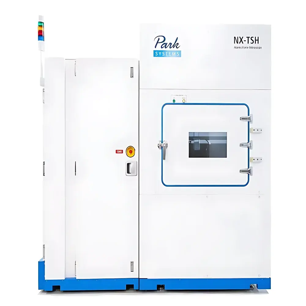
| Brand | Park SYSTEMS |
|---|---|
| Origin | South Korea |
| Model | NX-TSH |
| Instrument Type | Industrial AFM |
| Sample Stage Travel Range | 625 mm × 525 mm |
| Maximum Sample Dimensions | 520 mm × 520 mm × 10 mm (10 kg) |
| Acoustic Noise Attenuation | >20 dB with Integrated Acoustic Enclosure |
| XY Scanning Range (Closed-Loop) | 100 µm × 100 µm |
| Z Scanning Range | 15 µm |
| Z Sensor Noise Floor | Sub-nanometer (low-noise optical lever detection) |
| Probe Exchange | Automated Tip eXchanger (ATX) with vision-based tip recognition and magnetic probe handling |
| Laser Alignment | Motorized, auto-focused beam positioning |
| Electrostatic Control | Integrated bipolar ionizer for charge neutralization |
| Electrical Characterization Option | Conductive AFM (C-AFM) with micro-probe station and 2D encoder stage |
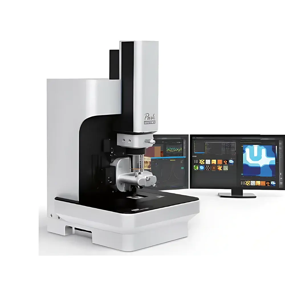
| Brand | Park SYSTEMS |
|---|---|
| Origin | Fujian, China |
| Manufacturer Type | Authorized Distributor |
| Origin Category | Domestic (China) |
| Model | NX10 High-Precision Atomic Force Microscope (SHNTI) |
| Price Range | USD 95,000 – 218,000 |
| Instrument Type | Atomic Force Microscope (AFM) |
| Application Class | Materials Science AFM |
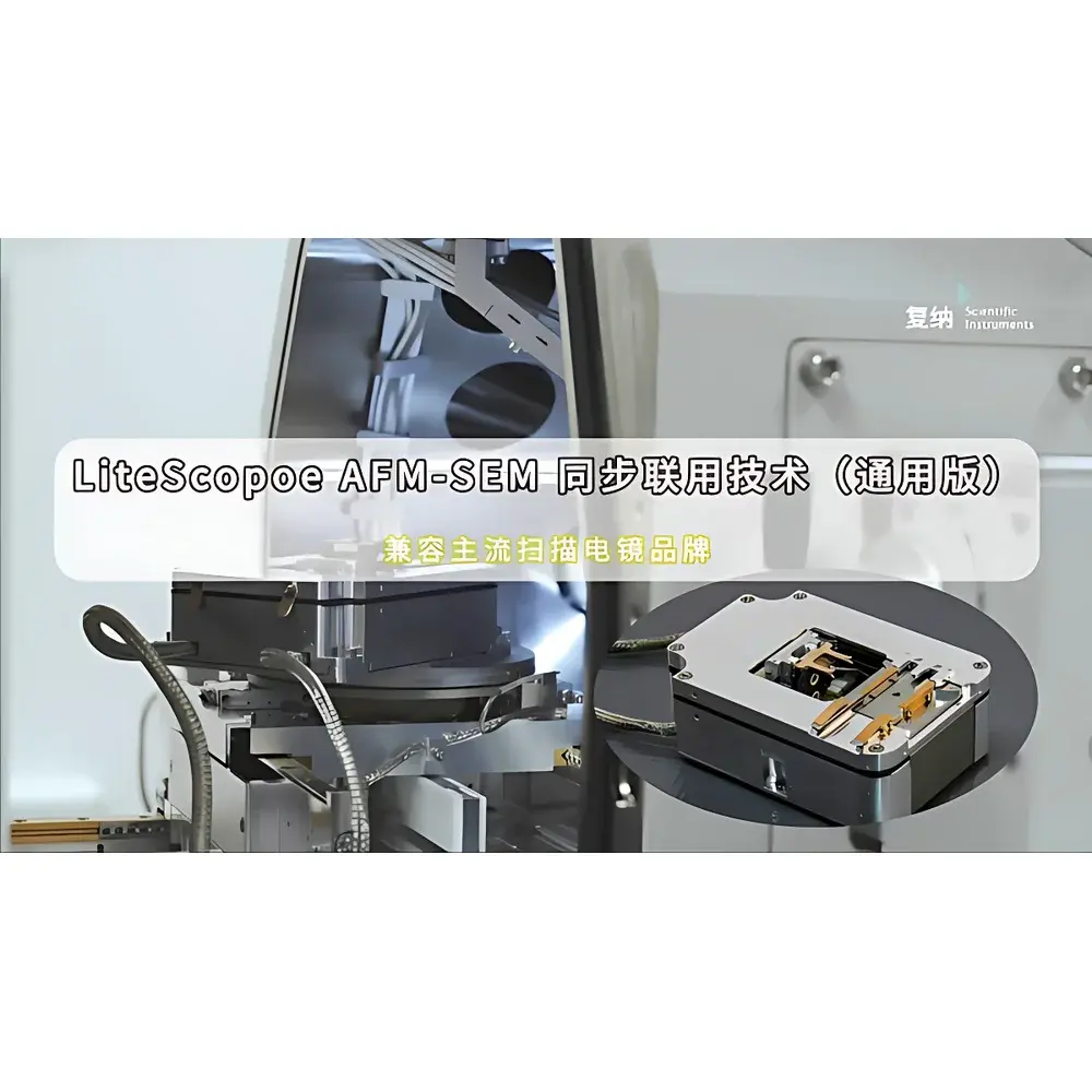
| Brand | Phenom |
|---|---|
| Origin | Netherlands |
| Manufacturer Type | Authorized Distributor |
| Origin Category | Imported |
| Model | LiteScope |
| Instrument Type | Atomic Force Microscope |
| Sample Dimensions | 21 mm × 11 mm × 8 mm |
| Closed-Loop Scan Range | 80 µm × 80 µm × 16 µm |
| Compatibility | Thermo Fisher, TESCAN, Zeiss, Hitachi, JEOL SEM platforms (custom integration available) |
| Measurement Modes | Contact/Non-contact AFM, Phase Imaging, Energy Dissipation Mapping, C-AFM, KPFM, EFM, STM, MFM, PFM, Force–Distance (F–z), Current–Voltage (I–V), CPEM Correlative Analysis |
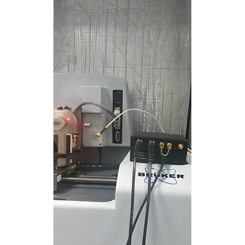
| Origin | USA |
|---|---|
| Manufacturer Type | Authorized Distributor |
| Origin Category | Imported |
| Model | Prime |
| Price Range | USD 135,000 – 205,000 |
| Instrument Type | Atomic Force Microscope (AFM)-Based Scanning Microwave Impedance Microscope |
| Positional Detection Noise | 0.01 nm |
| Scan Area | 20 µm × 20 µm (model-dependent) |
| Stage Travel Range | 100 µm × 100 µm × 10 µm |
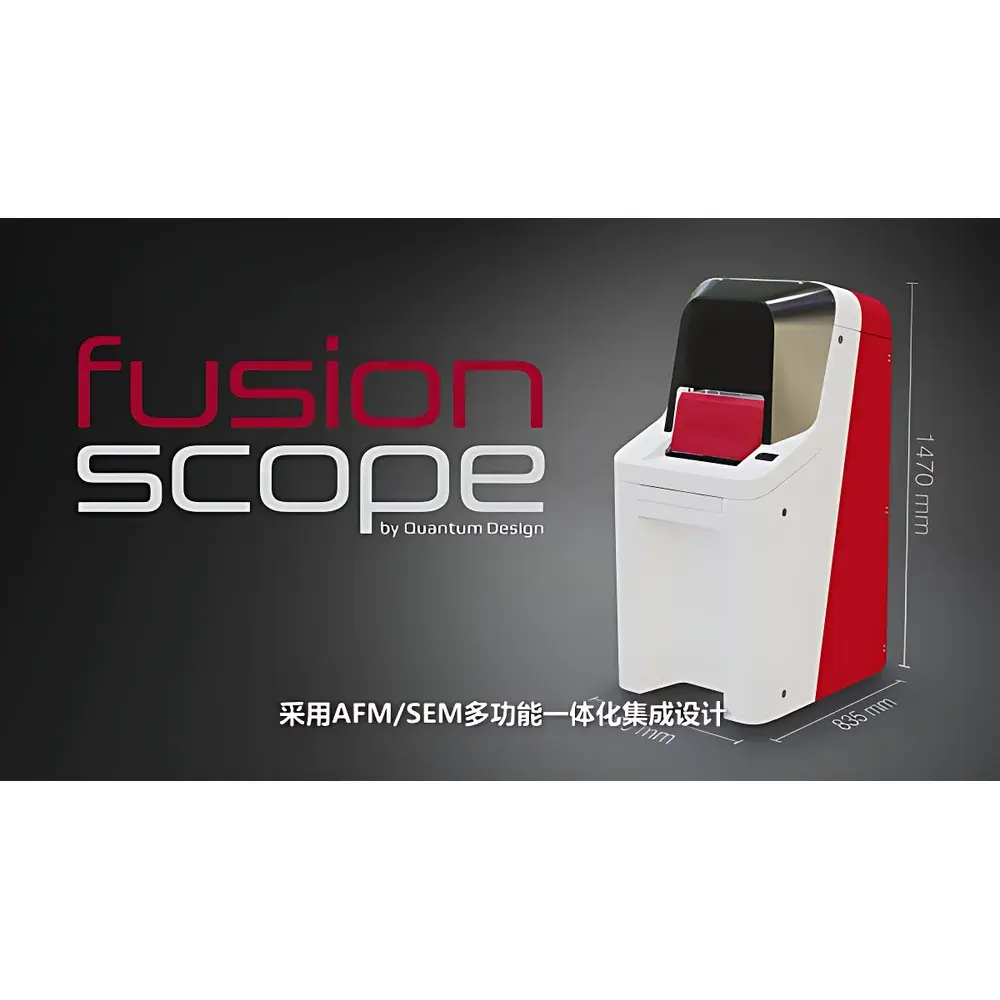
| Brand | Quantum Design |
|---|---|
| Origin | USA |
| Manufacturer Type | Original Equipment Manufacturer (OEM) |
| Product Category | Imported Instrument |
| Model | FusionScope |
| Instrument Type | Materials-Focused Hybrid AFM/SEM System |
| Positional Detection Noise | <50 pm @ 1 kHz |
| Maximum Sample Diameter | ≤20 mm |
| Maximum Sample Height | ≤20 mm |
| Sample Stage Travel Range | XY: 22 × 22 µm (closed-loop), Z: 15 µm |
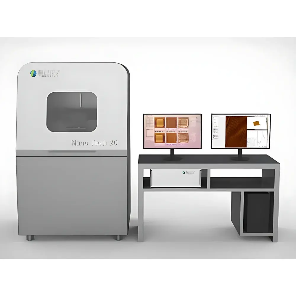
| Brand | Quantum Scale |
|---|---|
| Origin | Jiangsu, China |
| Manufacturer Type | Authorized Distributor |
| Product Category | Domestic |
| Model | Nano Tech 20 AFM |
| Instrument Type | Industrial-Grade |
| SPM Architecture | Modular & Multi-Functional |
| Positioning Noise | XY: 0.2 nm, Z: 0.05 nm |
| Sample Size Compatibility | Up to 300 mm (12-inch) wafers, downward-compatible |
| XY Stage Travel | 200 mm × 200 mm (customizable) |
| Z Scan Range | 10 µm |
| Imaging Modes | Contact, Tapping, Force Spectroscopy, Phase Imaging |
| Optional Upgrades | EFM, MFM, KPFM, PFM, Lateral Force Imaging |
| Optical Microscope | 6.3 MP color CMOS, 7.5×–50× zoom, 34 mm working distance, 1.5 µm optical resolution at 50×, coaxial LED illumination, parfocal design |
| Scan Speed | 0.1–20 Hz |
| Feedback Bandwidth | 500 kHz (dual-channel lock-in), 18-bit amplitude/phase resolution |
| Data Acquisition | 16-bit, 100 kHz multi-channel sampling |
| Environmental Options | Vacuum mode (7.3 Pa base pressure), inert gas enclosure (N₂/Ar), H₂O/O₂ monitoring, temperature-controlled stage (−100 °C to +150 °C, ±0.3 °C stability), active air-sound shielding, pneumatic vibration isolation platform |
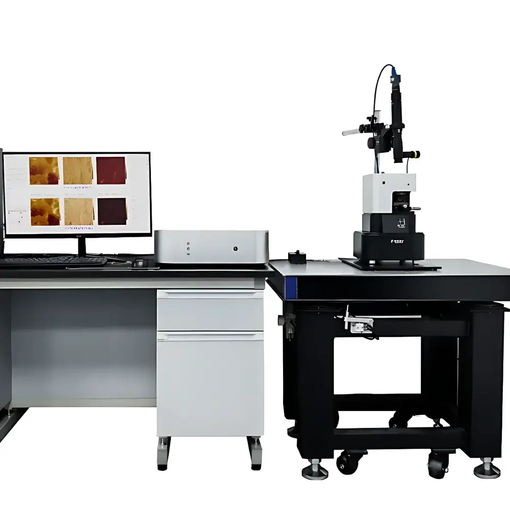
| Brand | Quantum Scale |
|---|---|
| Origin | Jiangsu, China |
| Manufacturer Type | Authorized Distributor |
| Product Category | Domestic |
| Model | NanoTech 10 AFM |
| Instrument Type | Materials-Focused AFM |
| SPM Architecture | Modular & Multi-Functional |
| Closed-Loop Positioning Noise | XY = 0.2 nm, Z = 0.05 nm |
| Sample Dimensions | 25 mm × 10 mm |
| XY Scanner Travel Range | 12 mm × 12 mm |
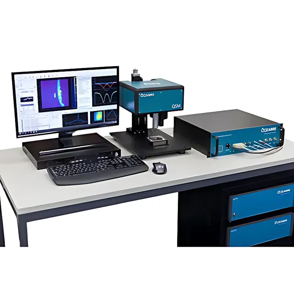
| Brand | Qzabre |
|---|---|
| Origin | Switzerland |
| Manufacturer Type | Authorized Distributor |
| Origin Category | Imported |
| Model | QSM |
| Instrument Type | Magnetic Force Microscope (MFM) |
| Positional Drift Rate | 6 nm/h |
| Sample Size | 25 mm diameter (standard) |
| Scan Range | 90 μm × 90 μm × 15 μm (closed-loop, 0.15 nm resolution) |
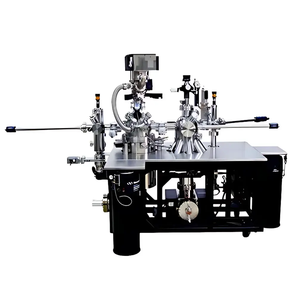
| Brand | RHK |
|---|---|
| Origin | USA |
| Manufacturer Type | Authorized Distributor |
| Origin Category | Imported |
| Model | QuadraProbe |
| Instrument Type | Scanning Tunneling Microscope (STM) |
| Sample Stage Travel Range | 1.5 µm (300 K) |
| Sample Temperature | 10 K (LHe), 80 K (LN₂) |
| Coarse Approach Range (X/Y/Z) | ±1.5 mm per step |
| Sample Positioning Accuracy | ±1.5 mm |
| STM Resolution | Atomic resolution on HOPG achievable with all four probes |
| SEM Resolution | <20 nm |
| Probe Material | Tungsten wire, optionally coated with Pt, Au, or other conductive metals |
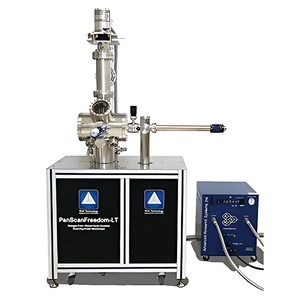
| Brand | RHK Technology |
|---|---|
| Origin | USA |
| Model | PanScan Freedom STM/qPlus AFM |
| Instrument Type | Ultra-High Vacuum Scanning Tunneling Microscope / qPlus Atomic Force Microscope |
| Position Detection Noise | <1 pm |
| Sample Size | 10 × 10 mm |
| Coarse XYZ Travel Range (RT) | 5 × 5 × 8 mm |
| Fine Scan Range (15 K) | 2 × 2 × 0.5 µm |
| Operating Temperature Range | 9 K – 400 K |
| XY Drift | 0.2 Å/hour |
| Z Drift | 0.2 Å/day |
| Magnetic Field Options | 5 T perpendicular or 1 T vector field (in-plane) |
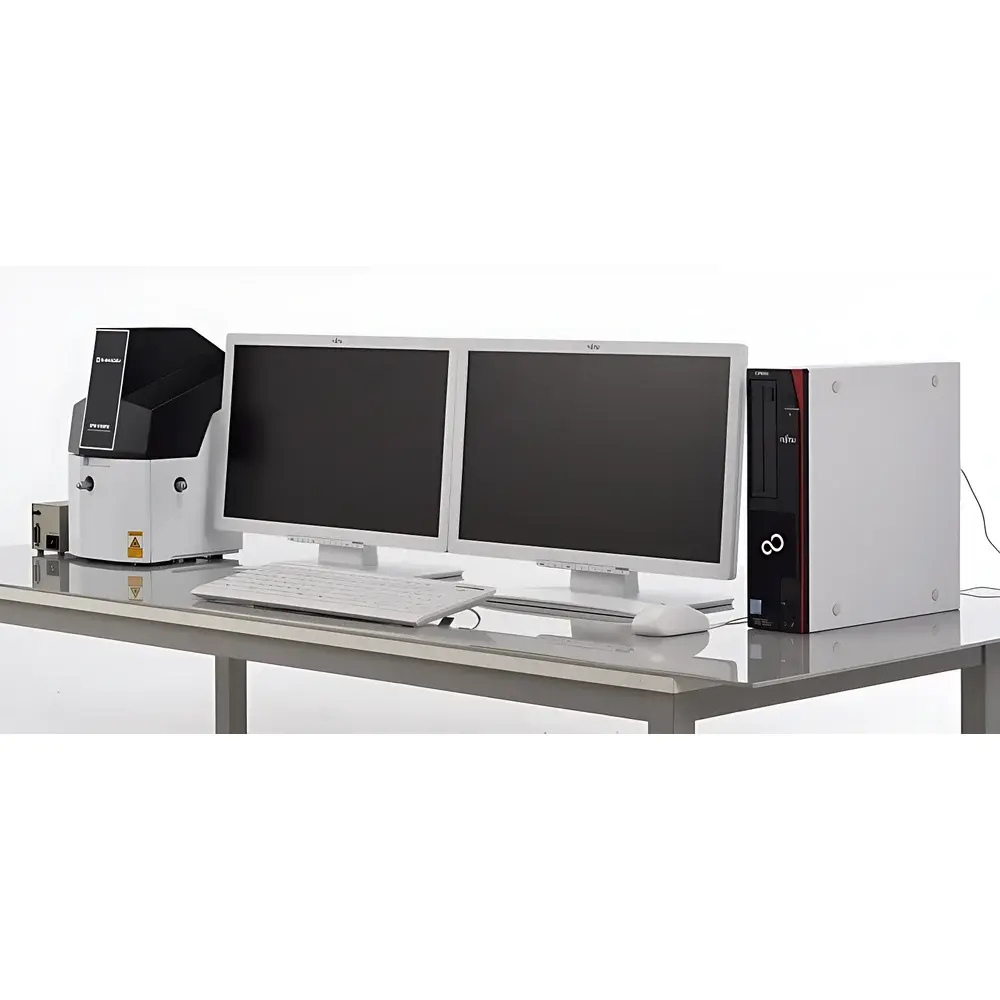
| Brand | Shimadzu |
|---|---|
| Origin | Japan |
| Manufacturer Type | Original Equipment Manufacturer (OEM) |
| Product Origin | Imported |
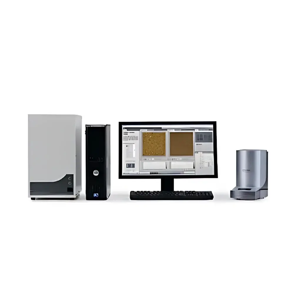
| Model | SPM-8100FM |
| Instrument Type | Atomic Force Microscope (AFM) |
| Lateral Positioning Noise | 0.1 nm |
| Vertical Positioning Noise | 0.03 nm |
| Sample Diameter × Thickness | Φ24 mm × 8 mm |
| Sample Stage Travel Range | ±5 mm |
| Brand | Shimadzu |
|---|---|
| Origin | Japan |
| Manufacturer Type | Original Equipment Manufacturer (OEM) |
| Product Category | Imported Instrument |
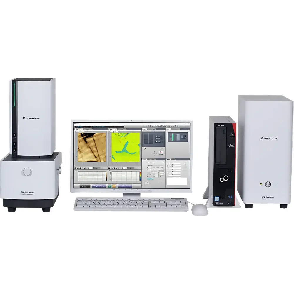
| Model | SPM-9700HT |
| Instrument Type | Atomic Force Microscope (AFM) |
| XY Positioning Noise | 0.1–0.2 nm (horizontal) |
| Z Positioning Noise | 0.03–0.05 nm (vertical) |
| Sample Size | Ø24 mm × 8 mm |
| Sample Stage Travel Range | ±6 mm |
| Brand | Shimadzu |
|---|---|
| Origin | Japan |
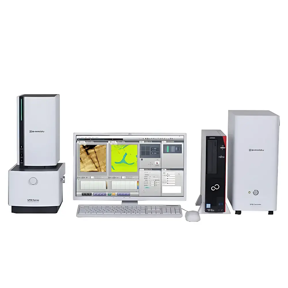
| Manufacturer | Shimadzu Corporation |
| Instrument Type | Atomic Force Microscope (AFM) |
| Category | Materials AFM |
| Position Detection Noise | < 0.02 nm RMS |
| Sample Dimensions | Ø50 mm × 8 mm max thickness |
| XY Stage Travel Range | 5 mm × 5 mm |
| Imaging Resolution | Up to 8192 × 8192 pixels |
| Automation Features | Auto-alignment ("Link On"), Auto-parameter optimization ("NanoAssist"), Fully automated tip exchange and fast 3D mapping |
| Brand | Shimadzu |
|---|---|
| Origin | Japan |
| Model | SPM-Nanoa |
| Instrument Type | Material-oriented AFM |
| Position Detection Noise | < 0.02 nm (RMS) |
| Sample Diameter | 50 mm |
| Sample Thickness | ≤ 8 mm |
| XY Stage Travel Range | 5 × 5 mm |

| Brand | SPIP |
|---|---|
| Origin | USA |
| Model | 6.0.14 |
| Distribution Type | Authorized Distributor |
| Import Status | Imported |
| Pricing | Available Upon Request |
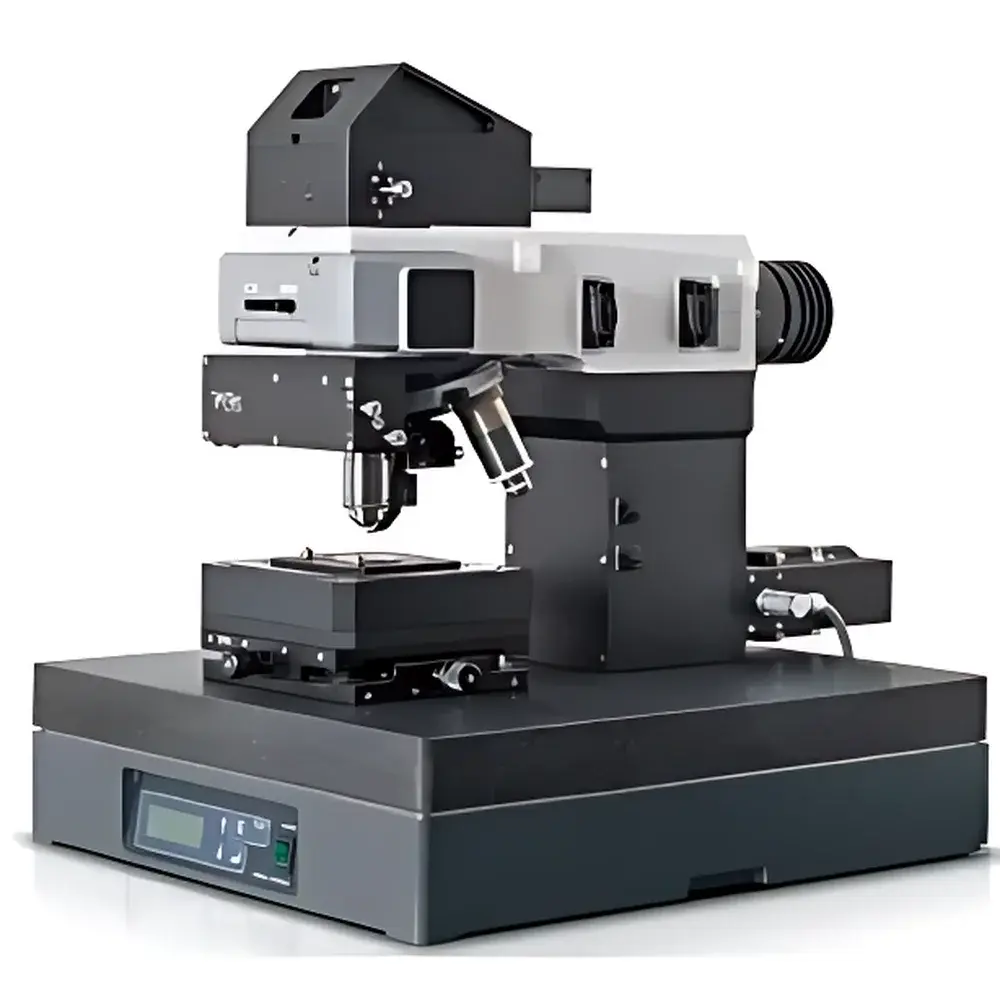
| Brand | Oxford Instruments |
|---|---|
| Origin | Germany |
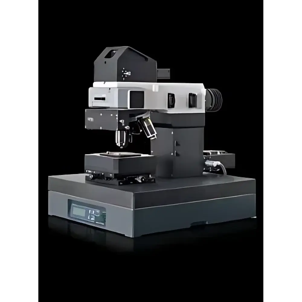
| Model | alpha300 A |
| Instrument Type | Materials-Focused AFM |
| Position Detection Noise | ≤0.5 nm |
| Maximum Sample Diameter | 120 mm |
| Piezo Scanner Travel Range (X/Y) | ≤100 µm |
| Integrated Microscopy | Research-Grade Optical Microscope with Brightfield, Darkfield, Polarization & Fluorescence Capabilities |
| Scanning Technology | TrueScan™ Capacitive Feedback-Controlled Stage |
| Brand | WITec |
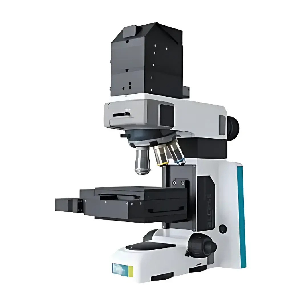
|---|---|
| Origin | Germany |
| Model | alpha300 A |
| Instrument Type | Atomic Force Microscope |
| Position Detection Noise | ≤0.5 nm |
| Sample Dimensions | Diameter < 15 mm, Thickness < 5 mm |
| Sample Stage Travel Range | ≤120 mm |
| Brand | WITec |
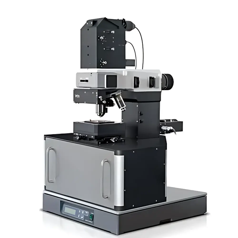
|---|---|
| Origin | Germany |
| Model | alpha300 access |
| Sample Diameter Limit | <15 mm |
| Sample Thickness Limit | <5 mm |
| XYZ Stage Travel Range | ≤120 mm |
| Positional Noise | 625 nm (RMS) |
| Instrument Type | Confocal Raman Microscope |
| Optical Architecture | Integrated UHTS High-Throughput Spectrometer |
| Microscope Platform | Precision-Engineered Inverted/Epifluorescence-Compatible Optical Microscope |
| Brand | WITec |
|---|---|
| Origin | Germany |
| Model | alpha300S |
| Sample Diameter | < 120 mm |
| Sample Thickness | < 25 mm |
| Scanner Range | 100 × 100 × 20 µm |
| Positioning Noise | RMS |
| Imaging Bandwidth | up to 625 Hz |
| Lateral Optical Resolution | ~60 nm |
| SNOM Mode Resolution | 50 nm |
| Confocal Raman Resolution | 200 nm |
| Detector Options | PMT or APD |
| Compatible Spectrometer | UHTS |