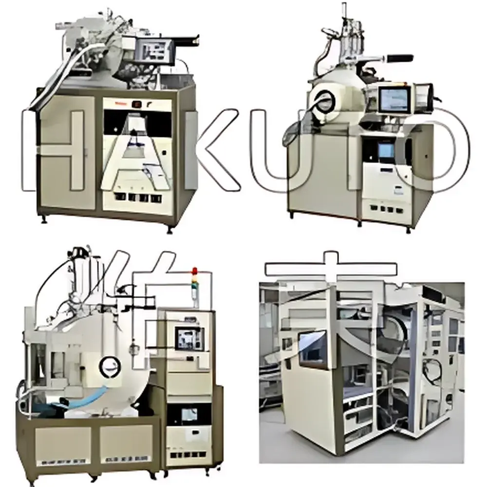
Hakuto IBE Series Ion Beam Etcher
| Brand | NS (Nippon Seiko) |
|---|---|
| Origin | Japan |
| Manufacturer Type | Authorized Distributor |
| Origin Category | Imported |
| Model | IBE |
| Price Range | USD 210,000 – 280,000 |
| Sample Diameter | 3"–6" φ |
| Max. Ion Incidence Angle | ±90° |
| Ion Source | Kaufman-type KDC-40 / KDC-75 / KDC-160 (KRI, USA) |
| Ultimate Vacuum | ≤1×10⁻⁴ Pa (4IBE/7.5IBE/16IBE/20IBE), ≤8×10⁻⁵ Pa (MEL 3100) |
| Turbomolecular Pump | Pfeiffer (350 L/s or 1250 L/s) |
| Etch Uniformity | ≤±5% |
| Cooling | Direct substrate cooling |
| Motion System | Dry Chuck Planet (planetary rotation + revolution) |
| Etch Mode | Physical sputtering (Ar⁺ beam), non-reactive, anisotropic |
Overview
The Hakuto IBE Series Ion Beam Etcher is a high-precision, physically driven dry etching system engineered for demanding research and pilot-scale semiconductor fabrication environments. Unlike chemically assisted plasma-based techniques such as Reactive Ion Etching (RIE), the IBE system employs a collimated, neutralized argon ion beam generated by a Kaufman-type ion source to perform purely physical sputter etching—enabling high-fidelity patterning of materials resistant to conventional reactive plasmas. This principle ensures exceptional process control over etch directionality, profile fidelity (vertical, angled, or tapered), and minimal chemical contamination—critical for spintronic devices, superconducting thin films, magnetic multilayers (e.g., CoFeB/MgO), noble metals (Au, Pt), and compound semiconductors (GaAs, InP, SiC). Designed and manufactured in Japan by NS (Nippon Seiko) under the Hakuto brand, the IBE platform has been deployed globally since 1970, with over 500 units installed across university cleanrooms, national laboratories, and advanced R&D facilities.
Key Features
- High-stability Kaufman ion sources (KDC-40, KDC-75, KDC-160) from Kimball Physics (USA), delivering controllable ion energy (100–1500 eV) and beam current density up to 1.5 mA/cm² for reproducible sputter yields.
- Ultra-high vacuum architecture featuring Pfeiffer turbomolecular pumps (350 L/s or 1250 L/s) and all-metal sealing, achieving base pressures ≤1×10⁻⁴ Pa (≤8×10⁻⁵ Pa on MEL 3100 variant) to minimize residual gas interactions and ensure stoichiometric etch fidelity.
- Dry Chuck Planet sample stage: combines synchronized planetary rotation and revolution to eliminate shadowing effects and achieve ≤±5% etch uniformity across 3″–6″ wafers—even on patterned or topographically complex substrates.
- Direct substrate cooling via liquid-nitrogen or closed-loop chiller interface, enabling low-temperature etching (<−100°C) to suppress surface diffusion, reduce redeposition, and preserve crystallinity in temperature-sensitive layers.
- Modular chamber design supporting variable ion incidence angles (0° to ±90°), facilitating controlled sidewall tapering, lift-off compatibility, and ion-assisted deposition (IAD) integration.
Sample Compatibility & Compliance
The IBE system demonstrates broad material compatibility without requiring process-specific chemistry optimization: it reliably etches hard metals (Pt, Au, NiFe, CoCr), insulators (Al₂O₃, SiO₂, MgO), superconductors (YBCO, NbN), and III–V/II–VI compound semiconductors—materials often unresponsive or poorly controlled in RIE. Its physical sputtering mechanism eliminates fluorine- or chlorine-based residues, making it compliant with stringent requirements for MRAM, SQUID sensors, and quantum device fabrication. The system adheres to ISO 14644-1 Class 5 cleanroom integration standards and supports GLP/GMP-aligned operation through configurable log archiving and hardware interlocks. While not certified to FDA 21 CFR Part 11 out-of-the-box, its software architecture permits audit-trail implementation for regulated environments upon customer specification.
Software & Data Management
Control is executed via a real-time Windows-based HMI with deterministic I/O response (<10 ms loop time), supporting programmable ramping of beam voltage, current, and stage motion parameters. All process recipes—including ion energy, beam current, exposure time, angle sequence, and cooling setpoint—are stored with timestamped metadata and user authentication. Raw sensor data (ion gauge pressure, thermocouple readings, pump status, beam current feedback) are logged at 1 Hz resolution and exportable in CSV or HDF5 format. Optional Ethernet/IP and Modbus TCP interfaces enable integration into factory MES systems for traceability in pilot-line settings.
Applications
- Spintronics: Patterning of magnetic tunnel junctions (MTJs), spin valves, and exchange-biased stacks with atomic-layer precision and no interfacial oxidation.
- MEMS & NEMS: High-aspect-ratio etching of Si, SiC, and diamond for resonators, gyroscopes, and nanomechanical sensors.
- Optoelectronics: Fabrication of distributed Bragg reflectors (DBRs), photonic crystal slabs, and ridge waveguides in GaN and InP with sub-10 nm edge roughness.
- Superconducting electronics: Definition of Nb, NbN, and MgB₂ Josephson junctions and kinetic inductance detectors (KIDs) without plasma-induced damage.
- Thin-film head manufacturing: Critical dimension control for GMR/TMR read elements and write pole structures in HDD development.
FAQ
What distinguishes ion beam etching (IBE) from reactive ion etching (RIE)?
IBE relies solely on physical sputtering using inert-gas ions (typically Ar⁺), offering superior selectivity independence, minimal chemical residue, and precise directional control—ideal for materials that lack volatile reaction products in RIE chemistries.
Can the IBE system perform angled or tilted etching?
Yes. The ion beam incidence angle is fully adjustable from 0° to ±90° relative to the substrate normal, enabling controlled sidewall profiles, undercut-free lift-off, and ion channeling studies.
Is the system compatible with cryogenic etching?
Yes. The direct-cooling substrate holder supports LN₂ or chiller-based thermal management down to −150°C, critical for suppressing defect migration in low-dimensional materials.
What vacuum performance is required for stable ion beam operation?
A base pressure ≤1×10⁻⁴ Pa is maintained using Pfeiffer turbomolecular pumps; lower base pressures (≤8×10⁻⁵ Pa) are achieved on the MEL 3100 configuration to minimize beam scattering and improve etch rate stability.
Does the system support automated batch processing?
The MEL 3100 and 20IBE-C variants include load-lock integration and robotic wafer handling, enabling unattended multi-wafer runs with full recipe recall and interlock safety monitoring.


