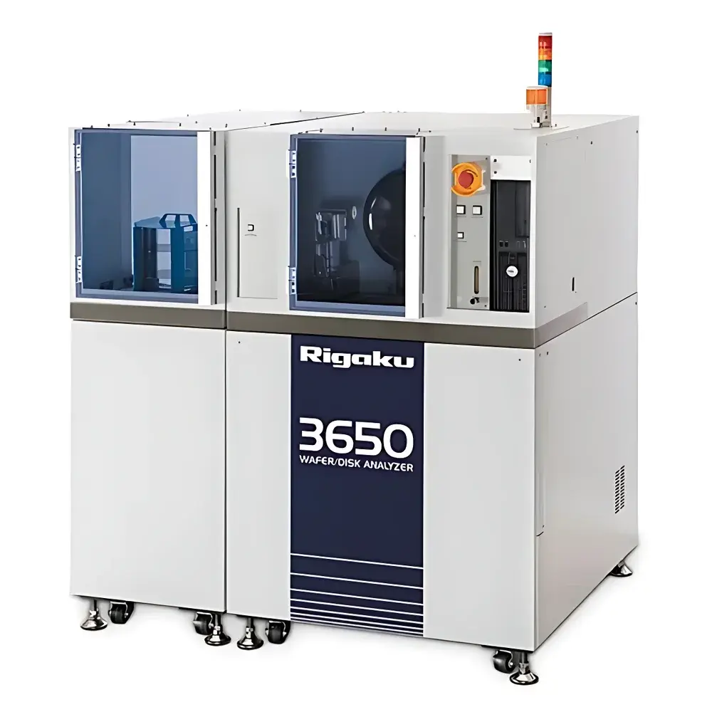
Rigaku WDA-3650 Wavelength Dispersive X-Ray Fluorescence Spectrometer
| Brand | Rigaku |
|---|---|
| Origin | Japan |
| Model | WDA-3650 |
| Instrument Type | Floor-standing |
| X-ray Tube Power | 4 kW |
| Elemental Range | Be (4) to U (92) |
| Detector Configuration | High-sensitivity AD-Boron channel for boron analysis |
| Instrument Architecture | Hybrid scanning + fixed-channel (multi-channel) WD-XRF |
| Sample Compatibility | Up to 200 mm wafers and magnetic/optical disks |
| Automation | Fully automated daily calibration (AutoCal), C-to-C robotic handler compatible (optional), SECS/GEM interface support |
| Vacuum & Thermal Stability | Integrated vacuum stabilization and active cooling systems |
| Footprint | 1.12 m (W) × 1.45 m (H) × 0.89 m (D) |
| Mass | 600 kg |
| Power Supply | 3-phase 200 VAC 50/60 Hz, 30 A or single-phase 220–230 VAC 50/60 Hz, 40 A |
| Regulatory Compliance | Designed for GLP/GMP environments |
Overview
The Rigaku WDA-3650 is a high-performance, floor-standing wavelength dispersive X-ray fluorescence (WD-XRF) spectrometer engineered for quantitative, non-destructive, and non-contact characterization of thin-film structures in semiconductor, data storage, and advanced materials manufacturing. Based on Bragg diffraction principles, the instrument utilizes crystal monochromators to resolve characteristic X-ray emission lines with high spectral resolution—enabling precise separation of overlapping peaks from adjacent elements (e.g., Si Kα and B Kα) and accurate quantification across the full elemental range from beryllium (Z = 4) to uranium (Z = 92). Its 4 kW Rh-anode X-ray source delivers exceptional photon flux, significantly enhancing detection sensitivity for light elements—particularly critical for boron quantification in BPSG films, dopant profiling in polycrystalline silicon, and trace-level impurity analysis in high-k dielectrics such as HfO₂ or Ta₂O₅.
Key Features
- Patented XYθZ motorized sample stage with sub-micron positioning repeatability, enabling high-accuracy mapping of film thickness and compositional uniformity across full 200 mm wafers without interference from diffraction artifacts—even for crystalline layers such as PZT, BST, or FeRAM stacks.
- Dual-mode optical architecture: Combines up to 20 fixed-channel analyzers (optimized for routine high-throughput measurement) with a high-resolution scanning spectrometer (Ti to U), offering flexibility for both production control and R&D-grade depth profiling.
- Dedicated AD-Boron detection channel featuring enhanced low-energy X-ray collection efficiency and optimized pulse processing, delivering sub-ppm detection limits for boron in oxide matrices under vacuum or helium purge conditions.
- Fully automated calibration system (AutoCal): Performs daily intensity normalization, PHA optimization, and background correction using certified reference wafers—eliminating manual intervention and ensuring long-term measurement stability across shifts and operators.
- Integrated vacuum stabilization and active thermal management subsystems maintain consistent detector gain and crystal lattice spacing, minimizing drift during extended acquisition sequences (e.g., multi-point wafer scans lasting >2 hours).
- SECS/GEM-compliant interface with CIM/FA protocol support enables seamless integration into automated fab environments; optional C-to-C robotic handler compatibility extends to SMIF POD and open cassette configurations.
Sample Compatibility & Compliance
The WDA-3650 accommodates standard 100 mm, 150 mm, and 200 mm semiconductor wafers, as well as magnetic media substrates (CoCrTa, CoCrPt), optical disks (Tb-FeCo), MRAM/TMR stacks, and MEMS-grade thin-film assemblies. Its robust mechanical design and vibration-damped optical bench meet ISO 14644-1 Class 5 cleanroom operational requirements. The system is architected for regulatory compliance in quality-critical environments: when operated with validated software and documented procedures, it supports audit-ready workflows aligned with ISO/IEC 17025, ASTM E1361 (standard test method for XRF analysis of thin films), and USP guidelines for elemental impurities. Full electronic records—including raw spectra, calibration logs, and operator actions—are retained with time-stamped, tamper-evident audit trails meeting FDA 21 CFR Part 11 criteria.
Software & Data Management
Control and analysis are executed via an embedded Windows®-based platform running Rigaku’s proprietary Quant’X software suite. The interface provides real-time spectrum visualization, multi-layer thin-film modeling (including matrix correction via fundamental parameters), and spatial distribution reporting (X-Y contour maps of thickness/composition). All analytical methods—including calibration curves, matrix correction coefficients, and measurement protocols—are stored in encrypted, version-controlled libraries. Raw spectral data adhere to ASTM E1301 and IUPAC-recommended formats, facilitating export to LIMS, MES, or statistical process control (SPC) platforms. Software validation packages—including IQ/OQ documentation, cybersecurity assessment reports, and change control logs—are available upon request for regulated users.
Applications
- Semiconductor process control: Thickness and stoichiometry of gate oxides (SiO₂, SiNₓ), silicides (WSiₓ, TiSi₂), barrier layers (TiN, TaN), and ferroelectric films (PZT, SBT).
- Dopant quantification: Boron in BPSG, phosphorus in PSG, arsenic in n-type polysilicon, and nitrogen in SiNₓ capping layers.
- Data storage R&D: Composition profiling of CoCr-based magnetic alloys, DLC overcoats, NiP underlayers, and GMR/TMR multilayer stacks.
- Advanced packaging: Intermetallic compound (IMC) analysis at Cu/Sn-Ag solder interfaces, thickness verification of redistribution layers (RDLs), and contamination screening for Cu, Ni, and Pb.
- Photovoltaics and display technologies: CdTe absorber layer stoichiometry, ITO transparency layer composition, and perovskite precursor film homogeneity assessment.
FAQ
What is the minimum detectable limit for boron using the AD-Boron channel?
Boron detection limits are typically ≤0.05 wt% in SiO₂-based matrices under optimized vacuum conditions and 1000 s counting time—dependent on film thickness, substrate composition, and spectral background.
Does the WDA-3650 support analysis of patterned wafers or structured substrates?
Yes—the XYθZ stage allows user-defined coordinate sets and automatic feature recognition via integrated camera alignment; measurements can be targeted to specific die, scribe lanes, or metrology pads.
Is vacuum required for light-element analysis?
Vacuum operation (<10 Pa) is recommended for Be–F quantification; helium flush mode is available as an alternative for Na–Mg analysis in ambient-compatible configurations.
Can the system perform depth-resolved analysis of multilayer stacks?
While not a true depth-profiling technique like SIMS or XPS, the WDA-3650 enables non-destructive thickness and composition determination of up to 5-layer stacks using iterative fundamental parameter modeling and angular-dependent excitation geometry.
What maintenance intervals are recommended for the 4 kW X-ray generator?
The Rh-anode tube has a rated lifetime of ≥2,000 hours under standard operating conditions; preventive maintenance—including crystal alignment verification and detector energy calibration—is recommended every 6 months or after 500 operating hours, whichever occurs first.