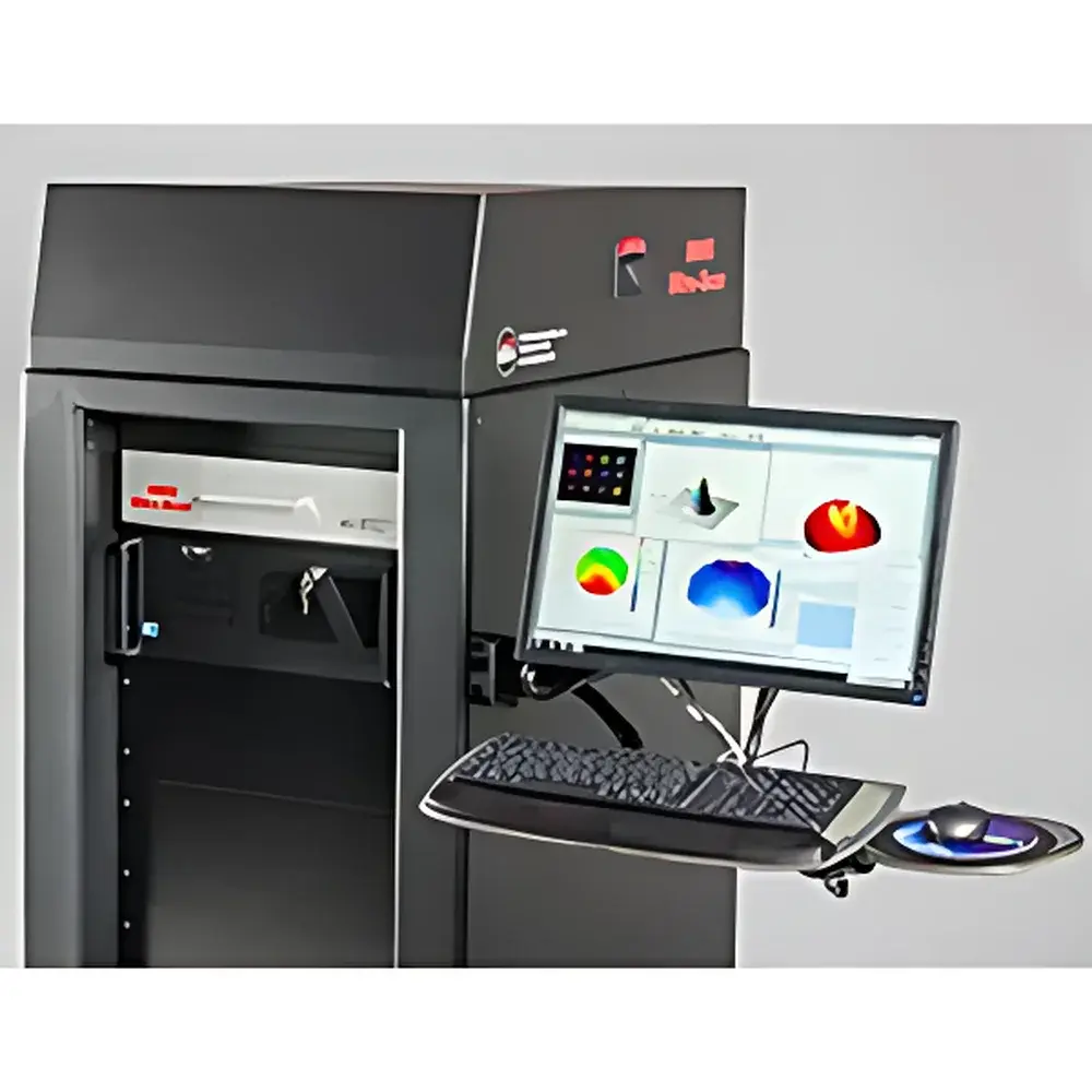
k-Space Associates kSA MOS US Thin-Film and Coating Residual Stress Analyzer
| Brand | k-Space Associates |
|---|---|
| Origin | USA |
| Model | kSA MOS US |
| Scan Area | 300 mm × 300 mm (up to 2 m optional) |
| Scanning Speed | up to 20 mm/s (X/Y) |
| Positional Resolution | 1 µm |
| Mean Curvature Resolution | 5 × 10⁻⁵ m⁻¹ (1σ) |
| Stress Measurement Range | 3.2 × 10⁵ Pa to 7.8 × 10⁹ Pa (1σ) |
| Stress Resolution | < 0.32 MPa or 1% (1σ) |
| Stress Repeatability | 0.02 MPa (1σ) |
| Curvature Repeatability | < 5 × 10⁻⁵ m⁻¹ (1σ) |
| Measurement Modes | Region-of-Interest, Linear Multi-Point, Full-Sample Scan |
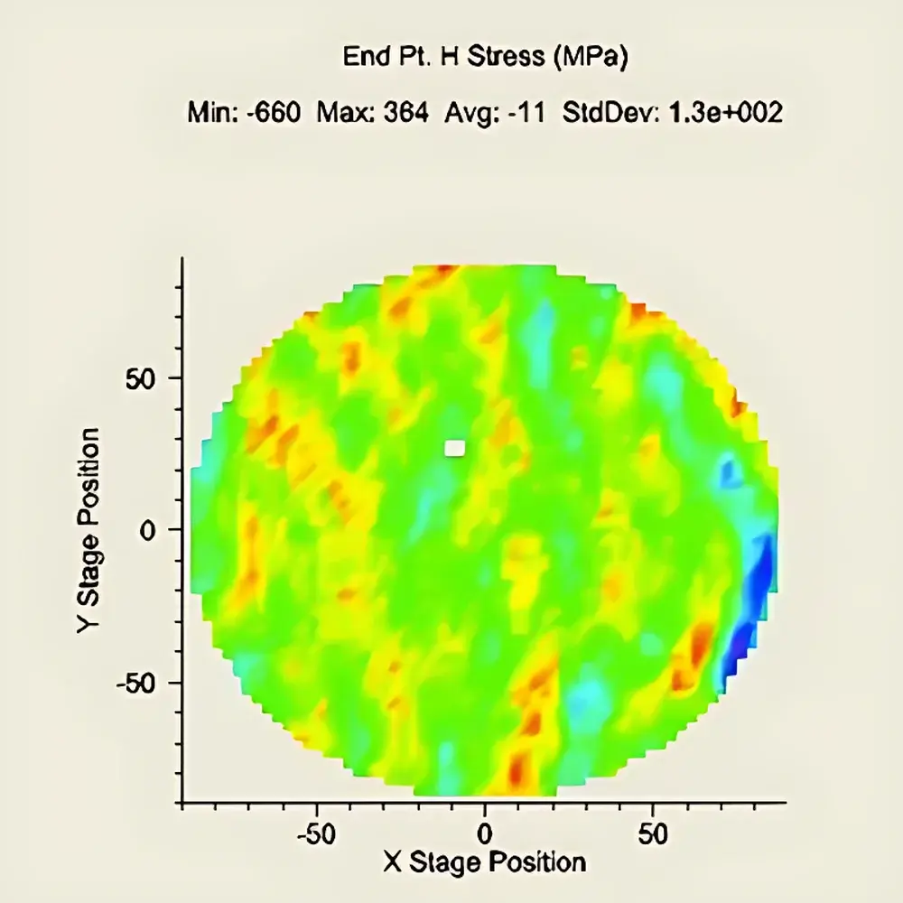
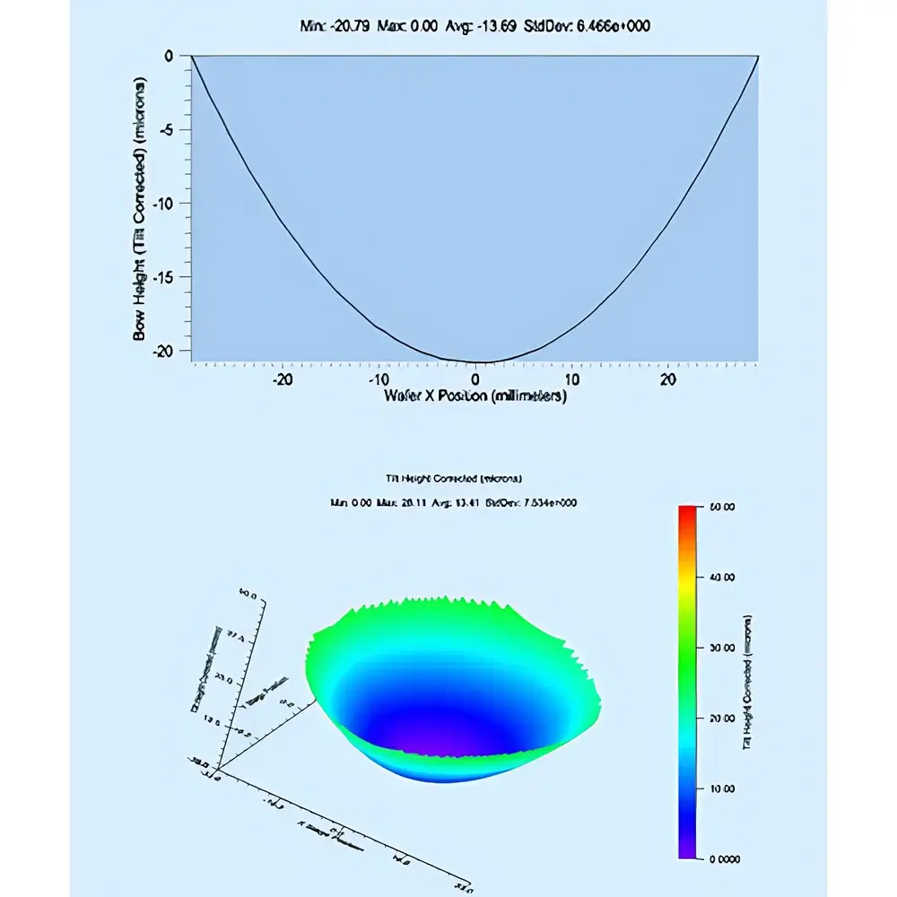
| Output | 2D curvature mapping, quantitative stress distribution imaging, radius of curvature, wafer bow, and stress intensity |
Overview
The k-Space Associates kSA MOS US Thin-Film and Coating Residual Stress Analyzer is a non-contact, high-precision metrology system engineered for quantitative characterization of mechanical stress in thin films and coatings deposited on rigid substrates. It operates on the principle of Multi-beam Optical Sensor (MOS) technology—a robust variant of Stoney’s equation-based curvature metrology—where an array of synchronized laser beams measures surface slope changes across a substrate with sub-microradian sensitivity. By detecting minute deviations in reflected beam angles from a polished surface, the instrument calculates local curvature, from which biaxial residual stress is derived using substrate mechanical properties and film thickness inputs. Unlike single-point profilometers or interferometric systems, the kSA MOS US employs a fixed two-dimensional laser array that scans without moving optics, eliminating vibration-induced phase noise and enabling stable, high-reproducibility measurements under ambient lab conditions. Designed for semiconductor wafers (Si, GaAs, SiC, sapphire), optical mirrors, precision lenses, display glass, and MEMS substrates, it delivers traceable, NIST-compatible curvature and stress data essential for process development, yield optimization, and reliability qualification.
Key Features
- Two-dimensional laser array architecture ensures simultaneous multi-point slope acquisition, eliminating scan-induced temporal artifacts and improving spatial coherence.
- Programmable XY translation stage with 1 µm positional resolution supports customizable measurement protocols: region-of-interest mapping, linear cross-sections, and full-area raster scans up to 300 mm × 300 mm (extendable to 2 m).
- Real-time curvature-to-stress conversion engine integrates user-defined substrate modulus, Poisson’s ratio, and film thickness to generate calibrated stress maps in MPa.
- Auto-alignment optical tracking compensates for minor sample tilt or thermal drift during extended acquisitions, maintaining measurement fidelity over hours-long thermal ramp sequences.
- Stress resolution better than 0.32 MPa (or 1% of reading) and repeatability of ±0.02 MPa (1σ) enable detection of low-magnitude stress gradients induced by annealing, plasma exposure, or interfacial reactions.
- Native support for thermal stress profiling via integrated environmental chamber interfaces—compatible with external ovens or cryostats for in-situ temperature-dependent curvature tracking from −100 °C to +400 °C.
Sample Compatibility & Compliance
The kSA MOS US accommodates flat, polished substrates with surface roughness < 1 nm RMS—including silicon wafers (50–300 mm diameter), fused silica optics, BK7 and CaF₂ lenses, borosilicate glass panels, and metal-coated mirrors. Its non-contact, non-destructive operation satisfies ISO/IEC 17025 requirements for accredited calibration labs and aligns with ASTM F390-22 (Standard Test Method for Measuring Residual Stress in Thin Films Using the Substrate Curvature Technique). Data acquisition workflows support audit-ready metadata tagging (operator ID, timestamp, environmental conditions), and raw curvature datasets are exportable in HDF5 and CSV formats for third-party statistical analysis. The system complies with CE marking directives (EMC 2014/30/EU, LVD 2014/35/EU) and meets FCC Part 15 Class A emission limits for laboratory deployment.
Software & Data Management
The proprietary kSA Analysis Suite provides a deterministic, scriptable environment for measurement control, real-time visualization, and post-processing. Users define custom scan patterns via intuitive graphical overlays or Python-based automation scripts (via included API). Stress maps are rendered in false-color 2D heatmaps with adjustable scaling, contour overlays, and line-profile extraction. Statistical tools include radial averaging, quadrant segmentation, and Zernike polynomial decomposition for aberration quantification. All measurement sessions log full parameter sets—including laser power, integration time, stage position history, and environmental sensor readings (optional temperature/humidity)—enabling full GLP/GMP traceability. Export modules support direct integration with JMP, MATLAB, and Python-based analytics pipelines. Audit trails comply with FDA 21 CFR Part 11 when paired with network-authenticated user accounts and electronic signature validation.
Applications
- Process development and qualification of PVD, CVD, ALD, and electroplated films in semiconductor front-end and back-end-of-line manufacturing.
- Thermal stress modeling validation for heterogeneous integration stacks (e.g., Si-on-insulator, GaN-on-Si, TSV redistribution layers).
- Coating adhesion assessment via stress evolution monitoring before/after thermal cycling or humidity exposure per JEDEC JESD22-A104.
- Optical component certification—quantifying figure error contributions from anti-reflective, mirror, or filter coatings on telescope mirrors and lithography optics.
- MEMS packaging stress analysis, including wafer-level capping and hermetic seal integrity evaluation.
- Academic research in thin-film mechanics, phase transformation kinetics, and interfacial reaction thermodynamics across materials science, physics, and nanotechnology laboratories.
FAQ
What physical principle does the kSA MOS US use to measure stress?
It applies the Stoney equation framework, deriving biaxial stress from measured substrate curvature using multi-beam optical slope detection—no physical contact or substrate bending is required.
Can the system measure stress on non-circular or irregularly shaped samples?
Yes—custom scan boundaries can be defined via polygonal masking; curvature calculations are performed only within user-specified regions, supporting rectangular, elliptical, or freeform substrates.
Is temperature-controlled measurement supported natively?
The base system operates at ambient temperature; however, it integrates seamlessly with third-party environmental chambers via analog/digital I/O ports for synchronized thermal ramping and curvature logging.
How is calibration traceability maintained?
The system includes factory-certified curvature reference standards traceable to NIST SRM 2634a (flatness artifact); users may perform periodic verification using certified spherical or cylindrical calibration plates.
Does the software support automated pass/fail reporting for production environments?
Yes—threshold-based flagging rules can be embedded in measurement templates, generating PDF reports with annotated stress maps, statistical summaries, and compliance status indicators.
Related Products


