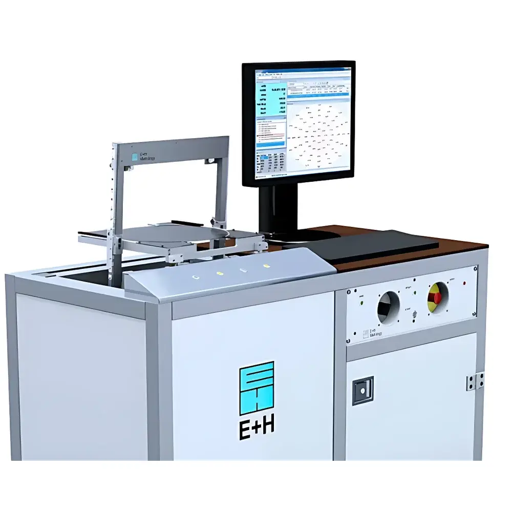
E+H Metrology MX 2012 Wafer Geometry Metrology System
| Brand | E+H Metrology |
|---|---|
| Origin | Germany |
| Manufacturer Type | Authorized Distributor |
| Origin Category | Imported |
| Model | MX 2012 |
| Pricing | Available Upon Request |
| Wafer Diameter | 300 mm (configurable for 200 mm) |
| Measurement Accuracy | ±0.5 µm |
| Resolution | 50 nm |
| Thickness Range | 500–1000 µm |
| Measurement Points | 69 |
| TTV (Total Thickness Variation) | Supported |
| Bow & Warp | Supported |
| Stress Evaluation | Optional |
| Measurement Orientation | Vertical (gravity-compensated) |
| Automation Level | Semi-automated (manual load/unload, automated measurement cycle) |
| Software | MX-NT |
| Sensor Principle | Capacitive displacement sensing |
| Probe Architecture | Dual orthogonal aluminum plates (1″ thick), each embedded with 69 capacitive sensors |
| Positioning Repeatability | ≤0.1 µm |
| Vacuum Fixture | Triple-circuit independent vacuum suction with dielectric-compensated polymer membrane |
Overview
The E+H Metrology MX 2012 Wafer Geometry Metrology System is a high-precision, vertically oriented metrology platform engineered for non-contact geometric characterization of silicon wafers up to 300 mm in diameter. It operates on the principle of differential capacitive displacement sensing—utilizing two rigid, orthogonal aluminum sensor plates (each 25.4 mm thick) embedded with 69 high-stability capacitive transducers per plate. The upper probe is pneumatically actuated via an eccentric cam mechanism driven by compressed air pistons, enabling precise vertical positioning with ≤0.1 µm repeatability. Crucially, measurements are performed in a vertical orientation to eliminate gravitational sag—ensuring mechanical stability and minimizing deformation-induced error during thickness, bow, and warp evaluation. The system supports full TTV (Total Thickness Variation), local thickness mapping, front-side bow, back-side warp, and optional residual stress estimation through curvature-based modeling. Designed for integration into semiconductor front-end process control environments, the MX 2012 meets foundational requirements for traceable, repeatable wafer geometry verification under ISO/IEC 17025-aligned laboratory practices.
Key Features
- Vertical measurement architecture eliminates gravity-induced wafer deflection, enabling sub-micron accuracy for bow and warp assessment.
- Dual 69-point capacitive sensor arrays mounted on thermally stable aluminum plates ensure uniform spatial sampling across full 300 mm wafer surfaces.
- Triple-zone independent vacuum chuck with dielectric-compensated polymer membrane ensures secure, low-distortion fixation without perturbing capacitance baseline calibration.
- Pneumatic eccentric lift mechanism provides deterministic, hysteresis-free vertical probe positioning with ≤0.1 µm mechanical repeatability.
- Configurable hardware and software support seamless transition between 300 mm and 200 mm wafer formats without recalibration.
- Integrated thermal drift compensation and real-time sensor linearity correction algorithms maintain measurement integrity over extended operational cycles.
Sample Compatibility & Compliance
The MX 2012 is validated for bare and oxide-coated silicon wafers (standard SEMI specifications), including prime, test, and monitor wafers with nominal thicknesses from 500 µm to 1000 µm. It complies with SEMI MF-1530 (Specification for Wafer Geometry Measurement) and supports data reporting formats compatible with SEMI E142 (Data Collection and Reporting Standard). While not certified as GMP or FDA 21 CFR Part 11 compliant out-of-the-box, the MX-NT software architecture permits audit trail configuration, user access controls, and electronic signature implementation when deployed within validated quality management systems. All calibration procedures follow traceable NIST-traceable reference standards and are documented per ISO/IEC 17025 clause 6.6.
Software & Data Management
The MX-NT control and analysis software provides full instrument orchestration, including probe sequencing, vacuum zone activation, sensor synchronization, and real-time thickness map generation. It supports ASTM E1089-compliant TTV calculation, ISO 10110-5-compliant surface form deviation analysis, and customizable report templates (PDF, CSV, XML). Raw sensor data—including individual channel offsets, temperature logs, and vacuum pressure traces—is retained with timestamped metadata. Data export interfaces comply with SECS/GEM protocol extensions for factory automation integration. Audit trails record all user actions, parameter changes, and calibration events with immutable timestamps—enabling compliance readiness for internal QA audits and external regulatory reviews.
Applications
- Front-end process monitoring: Pre- and post-CMP thickness uniformity verification and edge exclusion zone analysis.
- Epitaxial layer and SOI wafer qualification: Interface flatness assessment and buried oxide thickness consistency checks.
- Wafer warpage screening prior to lithography and bonding processes to prevent overlay errors.
- Residual stress profiling in strained-Si and SiGe heterostructures using curvature-to-stress conversion models.
- Reference standard certification in metrology labs supporting ISO/IEC 17025 accreditation scopes.
- Process tool matching studies across multiple CMP or epitaxy tools using inter-tool TTV and bow correlation metrics.
FAQ
What wafer diameters does the MX 2012 support?
The system is configured for 300 mm wafers as standard and can be reconfigured for 200 mm wafers via mechanical adapter kits and software parameter updates.
Is the MX-NT software qualified for regulated environments?
MX-NT is configurable for 21 CFR Part 11 compliance when deployed with appropriate IT infrastructure, role-based access controls, and electronic signature workflows—but requires site-specific validation per FDA guidance.
How is sensor drift compensated during long measurement sequences?
The system performs automatic zero-point referencing at the start of each measurement cycle using calibrated reference surfaces; real-time thermal compensation is applied based on integrated platinum RTD sensors embedded in both probe plates.
Can the MX 2012 measure patterned wafers?
Yes—provided topography features are within ±2 µm height variation and do not obstruct capacitive field coupling; measurement uncertainty increases for highly reflective or conductive metallization layers, and empirical validation is recommended per application.
What maintenance intervals are recommended for the vacuum system?
Vacuum filter elements require replacement every 6 months under continuous operation; polymer membrane inspection is advised quarterly, with replacement recommended after 12 months or 5,000 cycles, whichever occurs first.


