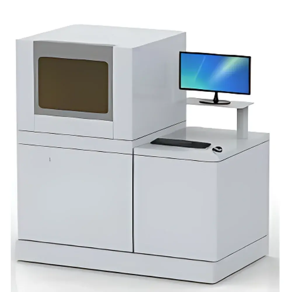
Holimatrix Holomatrix Holographic Nanoscale Photolithography Platform
| Origin | Hong Kong |
|---|---|
| Manufacturer Type | Authorized Distributor |
| Origin Category | Mainland China Made |
| Model | Holimatrix |
| Price Range | USD 140,000 – 210,000 |
Overview
The Holimatrix Holographic Nanoscale Photolithography Platform is a maskless, interference-based direct-write patterning system engineered for high-precision, large-area nanostructure fabrication on semiconductor wafers and functional substrates. Unlike conventional photolithography or electron-beam lithography systems, Holimatrix employs coherent two-beam laser interference at an optical interface—eliminating the need for physical masks, stamps, or electron optics. This approach leverages the fundamental principle of holographic lithography: spatially periodic intensity modulation generated by the superposition of two counter-propagating or angularly offset coherent beams. The resulting interference fringes define sub-wavelength periodic structures (down to <50 nm feature size) with exceptional uniformity and long-range order across 4-inch (100 mm) wafers. Its all-fiber-optic architecture—including a specialized single-mode fiber delivery system, integrated fiber beam splitter, and fiber-coupled spatial filtering at the output port—ensures mechanical stability, environmental insensitivity, and reproducible pattern registration. Closed-loop feedback control actively stabilizes the interference pattern in real time, enabling robust operation in standard laboratory environments without vibration isolation tables or temperature-controlled cleanrooms.
Key Features
- Maskless, mold-free holographic patterning—no photomasks, e-beam resists, or nanoimprint templates required
- Sub-50 nm minimum feature size with <±2.5% period accuracy across full 4-inch wafer field
- Programmable periodicity range: 200 nm to 2 µm—adjusted dynamically via software-controlled incident angle tuning
- All-fiber-optic interferometric setup: eliminates alignment drift, reduces sensitivity to air turbulence and thermal expansion
- Native compatibility with non-planar and warped substrates—supports wafers with up to 20 µm total indicator reading (TIR)
- Full automation via intuitive GUI: pattern selection, orientation, scaling, and exposure dose controlled via point-and-click interface
- Integrated closed-loop interferogram stabilization using piezo-driven path-length compensation and real-time fringe monitoring
Sample Compatibility & Compliance
The Holimatrix platform supports standard semiconductor substrates including silicon, sapphire (PSS), fused silica, SiC, GaN, and polymer films (e.g., PMMA, SU-8). It accommodates 4-inch (100 mm) wafers with optional upgrade paths for 6-inch handling. Pattern transfer is compatible with standard lift-off, etch, and nanoimprint processes. The system meets ISO 14644-1 Class 5 cleanroom operational requirements when used with laminar flow hoods. All optical components comply with IEC 60825-1:2014 (laser safety class 3B), and firmware implements audit-trail logging per FDA 21 CFR Part 11 guidelines for regulated R&D environments. Documentation includes traceable calibration certificates for beam alignment, exposure dose, and period verification.
Software & Data Management
Holimatrix Control Suite is a Windows-based application built on Qt framework with deterministic real-time scheduling for exposure sequencing. It provides vector-based pattern library management (1D gratings, 2D lattices, quasicrystals, and custom user-defined motifs), multi-layer overlay alignment using fiducial recognition, and dose mapping for resist-thickness compensation. Export formats include GDSII, SVG, and ASCII coordinate lists for downstream process integration. All session logs—including laser power, exposure time, stage position, environmental sensor readings (temperature/humidity), and operator ID—are timestamped and digitally signed. Data retention complies with GLP/GMP-aligned archival protocols, supporting full traceability from design to fabricated structure.
Applications
- Photonic device fabrication: photonic crystals, plasmonic metasurfaces, high-efficiency grating couplers, and subwavelength anti-reflection textures for solar cells
- LED and micro-LED manufacturing: patterned sapphire substrates (PSS), light-extraction enhancement structures, and directional emission control
- Nanopatterning for metrology: master gratings for CD-SEM calibration, scatterometry standards, and diffractive optical elements
- Functional surface engineering: superhydrophobic/philic textures, structural color generation, and SERS-active substrates
- Template synthesis: large-area nanoimprint molds for roll-to-roll and step-and-flash imprint lithography (S-FIL)
- Directed self-assembly (DSA) pre-patterning: chemical and topographic guiding templates with nanoscale registry
- Biosensor development: label-free plasmonic biosensor arrays and nanopore array substrates
FAQ
Does Holimatrix require vacuum or high-energy radiation sources?
No. It operates under ambient atmospheric conditions using visible or near-UV continuous-wave lasers—no vacuum chamber, electron gun, or X-ray source is involved.
Can it pattern on curved or flexible substrates?
Yes. Its optical interface design and adaptive focus algorithm support substrates with radii down to 50 mm curvature and thickness variations up to ±15 µm.
Is resist baking or post-exposure bake (PEB) integrated?
No. Holimatrix is a patterning tool only; standard hotplates or track systems are used for pre-bake and PEB as part of the broader process flow.
What resist types are validated for use with Holimatrix?
Standard positive-tone (e.g., AZ® 1518, ma-N 2403) and negative-tone (e.g., SU-8 2005, mr-I 8020) photoresists have been characterized for 365 nm and 405 nm exposure wavelengths.
How is system performance verified after installation?
A NIST-traceable calibration kit—including certified line-width standards and period reference gratings—is supplied, along with SOPs for daily interferogram stability checks and quarterly resolution validation.


