Norcada NHB-SNL In Situ Biasing and Heating System for Electron Microscopy
| Brand | Norcada |
|---|---|
| Origin | Canada |
| Model | NHB-SNL |
| Price Range | USD $45,000–$95,000 |
| Application Domain | Energy Storage & Battery Research |
| Instrument Type | In Situ Heating & Electrical Biasing Holder |
| Maximum Pressure | 100 Pa (compatible with TEM/SEM vacuum environments) |
| Current Measurement Range | pA to nA (configurable controller-dependent) |
| Temperature Range | Up to 1100 °C (in situ heating) |
| Voltage Range | Up to 40 V DC |
| Fluid Compatibility | Sealed MEMS cell design enables stable liquid/gas phase operation under high vacuum (≤10⁻⁵ mbar) |
Overview
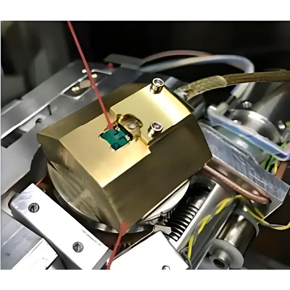
The Norcada NHB-SNL In Situ Biasing and Heating System is a dual-function, MEMS-based sample holder engineered for real-time structural, electrical, and thermal characterization inside scanning electron microscopes (SEM), transmission electron microscopes (TEM), and focused ion beam (FIB) systems. Leveraging monolithic silicon MEMS fabrication, the NHB-SNL integrates independently controllable heating and electrical biasing functionalities onto a single, compact platform compatible with standard Gatan, Oxford, or Protochips-style SEM/TEM holders. Its core measurement principle combines resistive Joule heating with four-terminal sensing architecture—enabling simultaneous nanoscale imaging and quantitative current–voltage (I–V) or resistance–temperature (R–T) analysis under controlled thermal conditions. Designed for high-reproducibility in situ experiments, the system supports dynamic studies of phase transformations, interfacial reactions, electrochemical solid–electrolyte interphase (SEI) evolution, and nanomaterial failure mechanisms under operational thermal and electrical stress.
Key Features
- Integrated dual-mode operation: Simultaneous or independent control of temperature (up to 1100 °C) and electrical bias (0–40 V DC) on a single MEMS chip
- Four-wire (Kelvin) measurement configuration ensures accurate pA–nA current resolution and eliminates lead resistance artifacts
- High-thermal-stability silicon nitride membrane window (thickness ≤ 50 nm) optimized for electron transparency and mechanical robustness
- Rapid thermal response: Achieves full heating/cooling cycles within 1 second across 0–1000 °C range without external water cooling
- Vacuum-compatible hermetic sealing enables stable liquid-phase (e.g., electrolyte droplets, ionic liquids) and gas-phase (e.g., H₂, O₂, CO₂) environments at pressures up to 100 Pa inside TEM/SEM columns
- Standardized mechanical interface compliant with ISO 80000-4 and ASTM E2736-19 for in situ holder interchangeability
Sample Compatibility & Compliance
The NHB-SNL accommodates diverse specimen geometries—including freestanding nanowires, thin-film heterostructures, battery electrode particles (up to 1 mm lateral dimension), and sealed liquid cells—without requiring custom stage modifications. Chip substrates are fabricated from low-background, electron-transparent SiN membranes with integrated Pt/Ti heater and electrode traces. All MEMS components meet RoHS Directive 2011/65/EU and are certified for use in Class 100 cleanroom environments. The system supports GLP-compliant experimental workflows: temperature calibration traceable to NIST SRM 1750a (chromel–alumel thermocouples), voltage/current outputs logged with 16-bit ADC resolution, and time-synchronized metadata tagging per frame acquisition (compatible with DigitalMicrograph™, Velox™, and EM-Monitor software APIs).
Software & Data Management
Norcada provides a modular LabVIEW-based control suite with optional Python SDK integration, enabling automated ramp-hold sequences, real-time I–V curve fitting (Ohmic, Schottky, Poole–Frenkel models), and synchronized acquisition triggers for EDS, EELS, or diffraction detectors. Data streams include timestamped thermal profiles, bias voltage sweeps, measured current, and optional external sensor inputs (e.g., pressure transducers, optical pyrometer signals). Audit trails comply with FDA 21 CFR Part 11 requirements when deployed with electronic signature-enabled configurations. Export formats include HDF5 (for machine learning training datasets), MRC (for tomography alignment), and CSV (for statistical process control in battery QA/QC labs).
Applications
- In situ TEM/SEM observation of Li-ion cathode degradation (e.g., oxygen release, transition metal migration) during electrochemical cycling at elevated temperatures
- Nanoscale Joule heating studies of graphene nanoribbon constrictions and phase-change memory devices
- Real-time imaging of solid–liquid interfacial dynamics in operando electrochemical cells (e.g., dendrite nucleation, bubble formation)
- Thermally activated defect migration in III–V semiconductors and 2D materials (MoS₂, h-BN) under bias
- FIB-assisted in situ annealing of implanted dopant profiles in SiGe heterojunctions
- Synchrotron XRD–TEM correlative studies of crystalline phase transitions in Ni-rich NMC under combined thermal–electrical stress
FAQ
Is the NHB-SNL compatible with both TEM and SEM platforms?
Yes—the holder uses standardized mechanical interfaces (e.g., double-tilt, single-tilt, or side-entry configurations) and has been validated on JEOL JEM-ARM300F, Thermo Fisher Talos F200X, Zeiss Sigma VP, and Hitachi SU5000 systems.
What vacuum levels support liquid-phase operation?
The sealed MEMS cell maintains integrity down to 10⁻⁵ mbar; liquid-phase experiments (e.g., aqueous electrolytes, ethylene carbonate–dimethyl carbonate blends) are routinely performed at 1–100 Pa using differential pumping or environmental TEM/SEM modes.
Can temperature and bias be ramped simultaneously while acquiring images?
Yes—real-time synchronization between thermal ramp profiles, voltage sweep parameters, and detector acquisition clocks is supported via TTL trigger outputs and software-defined timing constraints.
Does Norcada offer custom chip designs for proprietary electrode architectures?
Yes—custom MEMS layouts (e.g., interdigitated electrodes, microfluidic channels, multi-zone heaters) are available under NDA with lead times of 8–12 weeks and full process documentation per ISO 9001:2015.
How is temperature calibrated during in situ experiments?
Each chip undergoes factory calibration using reference thermocouples and blackbody radiation standards; users may perform in situ verification via electron energy loss spectroscopy (EELS) phonon peak shifts or diffraction ring contraction analysis.


