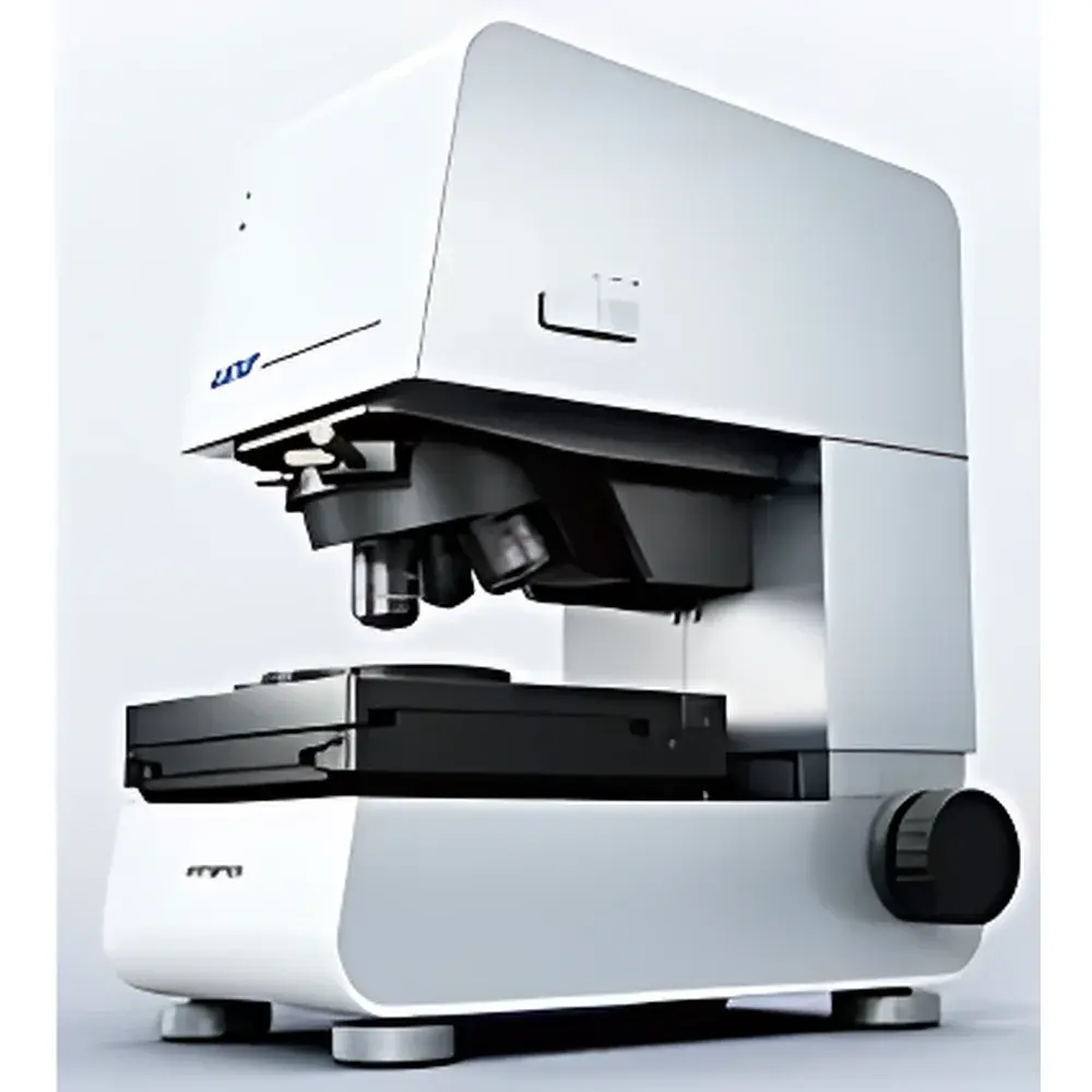
Olympus LEXT OLS4100 Laser Scanning Confocal Microscope
| Brand | Olympus |
|---|---|
| Origin | Japan |
| Model | LEXT OLS4100 |
| Type | Laser Scanning Confocal Microscope |
| Optical Resolution (XY) | 0.12 µm |
| Axial Resolution (Z) | 10 nm |
| Laser Wavelength | 405 nm |
| Detection System | Dual-Confocal Optical Architecture |
| Measurement Modes | 7 |
| Imaging Modes | Confocal, DIC-Laser (Laser Differential Interference Contrast), Multi-Layer Surface Analysis |
| Vibration Isolation | Integrated Composite Damping Mechanism (Spiral Spring + Damping Rubber) |
| Compliance | Designed for ISO/IEC 17025-aligned metrology workflows, supports GLP/GMP documentation traceability |
Overview
The Olympus LEXT OLS4100 is a high-precision laser scanning confocal microscope engineered for quantitative 3D surface metrology and non-destructive topographic imaging. Unlike conventional widefield or standard confocal microscopes optimized solely for fluorescence, the OLS4100 employs a dual-confocal optical architecture—combining two spatially separated pinholes with a high-sensitivity photodetector array—to achieve simultaneous depth discrimination and reflectance-independent contrast generation. This design enables robust, artifact-free height mapping across materials with highly variable surface reflectivity (e.g., bare silicon, gold-plated contacts, polymer films, and oxidized metals), without requiring conductive coating or vacuum environments. Its 405 nm violet diode laser source, coupled with high-numerical-aperture (NA) objective lenses, delivers lateral resolution down to 0.12 µm and axial resolution of 10 nm—performance validated per ISO 25178-601 for areal surface texture measurement. The system operates as a benchtop metrology instrument compliant with industrial QA/QC requirements in semiconductor fabrication, MEMS development, precision machining, and advanced materials R&D.
Key Features
- Dual-confocal optical path: Eliminates reflectivity-dependent signal saturation and enables consistent contrast across multi-material assemblies (e.g., solder bumps on Cu traces, SiN membranes over Si substrates).
- Multi-layer surface analysis mode: Quantifies individual interface heights and layer thicknesses in transparent or semi-transparent stacks (e.g., OLED encapsulation layers, anti-reflective coatings, PDMS microfluidic channels).
- Laser DIC (Differential Interference Contrast) mode: Generates pseudo-3D relief images with sub-10 nm height sensitivity, approximating SEM-level topographic fidelity without electron-beam charging artifacts.
- Macro-map navigation with real-time coordinate registration: Integrates low-magnification overview imaging with high-resolution scan positioning—enabling precise ROI selection across mm-scale samples without stage re-homing.
- Automated mosaic stitching: Supports programmable tile acquisition and geometrically corrected image fusion for seamless large-area (up to 100 × 100 mm) surface characterization.
- Integrated composite vibration isolation: Combines spiral spring suspension and viscoelastic damping rubber to suppress tabletop microvibrations (<0.5 µm RMS displacement at 1–100 Hz), eliminating the need for external optical tables in production lab environments.
- One-click reporting engine: Generates ISO/ASME-compliant measurement reports (including Sa, Sq, Sz, Sdr, Vmp) with embedded metadata, operator ID, timestamp, and calibration traceability logs.
Sample Compatibility & Compliance
The OLS4100 accommodates samples ranging from 10 mm × 10 mm wafers to 200 mm full-diameter semiconductor substrates (with optional motorized stage extension). It accepts non-conductive, reflective, translucent, and anisotropic surfaces—including uncoated Si, GaAs, sapphire, fused silica, PET films, electroplated Ni, and abraded Al₂O₃ ceramics—without sample preparation. The system adheres to ISO 25178-2 (areal surface texture parameters), ISO 1101 (geometrical product specifications), and ASTM E2927-19 (standard guide for 3D surface topography measurement using confocal microscopy). Audit trails, electronic signatures, and data integrity controls align with FDA 21 CFR Part 11 requirements when configured with Olympus’ certified software modules for regulated environments.
Software & Data Management
Olympus STREAM Metrology software provides a validated platform for measurement setup, real-time visualization, statistical process control (SPC) charting, and automated pass/fail evaluation against user-defined tolerances. Raw height maps (.xyz, .csv) and calibrated intensity data (.tif, .lsm) are stored with embedded EXIF-like metadata (laser power, scan speed, NA, Z-step, calibration certificate ID). Version-controlled project files support collaborative review and regulatory audit readiness. Optional integration with LabVantage LIMS or SAP QM modules enables direct transfer of measurement results into enterprise quality databases.
Applications
- Semiconductor: Wafer bump height uniformity, lithographic resist profile analysis, laser-drilled via depth consistency, TSV (through-silicon via) sidewall roughness quantification.
- MEMS & Precision Optics: Microlens array sag error, DMD mirror tilt angle deviation, MOEMS actuator stroke repeatability, anti-reflective coating thickness gradients.
- Advanced Manufacturing: Electroplated diamond tool wear profiling, wire bonding crater depth assessment, flexible PCB conductor edge roughness (Ra < 50 nm), thermal interface material (TIM) void fraction mapping.
- Materials Science: Abrasive grit distribution analysis (e.g., #400 sandpaper 3D morphology), carbon fiber tow surface waviness, textile yarn interlock geometry, hydrogel swelling kinetics via time-lapse Z-stack registration.
FAQ
Does the OLS4100 require vacuum or conductive coating for non-metallic samples?
No. Its confocal reflectance imaging mechanism operates in ambient air and does not rely on secondary electron emission—making it suitable for insulators, polymers, and biological tissues without metallization.
How is measurement traceability maintained across instrument lifecycles?
Each unit ships with NIST-traceable step-height standards and a factory calibration certificate. In-field verification is supported via Olympus-certified reference artifacts with documented uncertainty budgets per ISO/IEC 17025.
Can the system perform automated defect classification based on height thresholds?
Yes. STREAM Metrology supports rule-based binning logic (e.g., “flag all features > 2 µm height within 50 µm of bond pad edge”) with exportable CSV logs for SPC integration.
What is the maximum usable field of view at highest lateral resolution?
At 100× objective (NA 0.95), the single-frame FOV is 112 × 112 µm; mosaic stitching extends effective FOV to ≥100 mm while preserving pixel-level metrological integrity.
Is DIC-Laser mode compatible with quantitative height measurement?
DIC-Laser provides qualitative topographic contrast enhancement only. Quantitative Z-data is acquired exclusively in confocal or multi-layer mode using calibrated Z-scanning.


