FemtoTools FT-RS / FT-FS / FT-S / FT-G / FT-UMS1000 Nanoindenter and Micromanipulation System
| Brand | SHNTI (Distributor) |
|---|---|
| Origin | Switzerland |
| Model Series | FT-RS / FT-FS / FT-S / FT-G / FT-UMS1000 |
| Instrument Type | Nanoindentation and Scratch Tester |
| Maximum Indentation Depth | 1 µm |
| Effective Load Range | 5 nN – 10 mN |
| Load Resolution | 1 nN |
| Displacement Range | ±100 µm |
| Displacement Resolution | 5 nm |
| Maximum Friction Force | 1 mN |
| Indenter Tip Types | Berkovich, Cube-Corner, Flat Punch, Spherical (customizable) |
| Thermal Drift | <0.1 nm/s (at 25 °C, stabilized environment) |
Overview
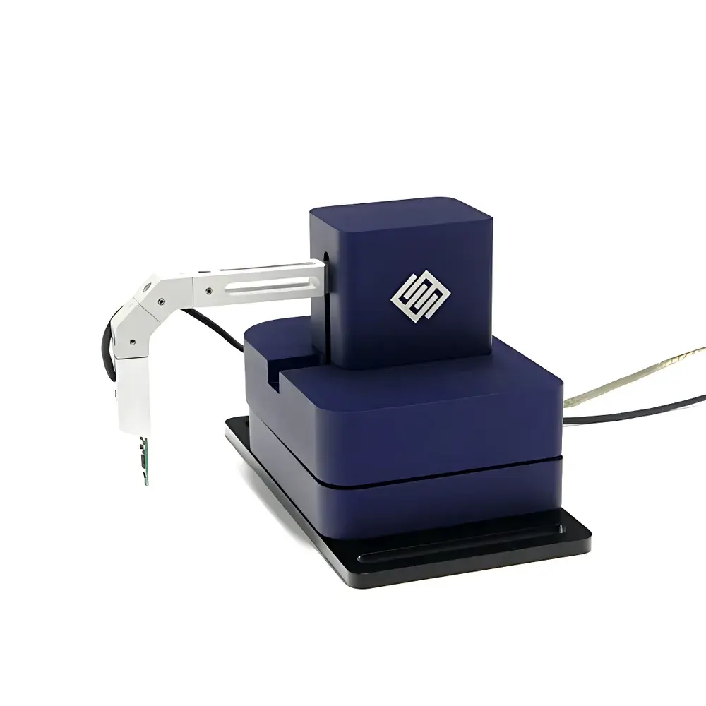
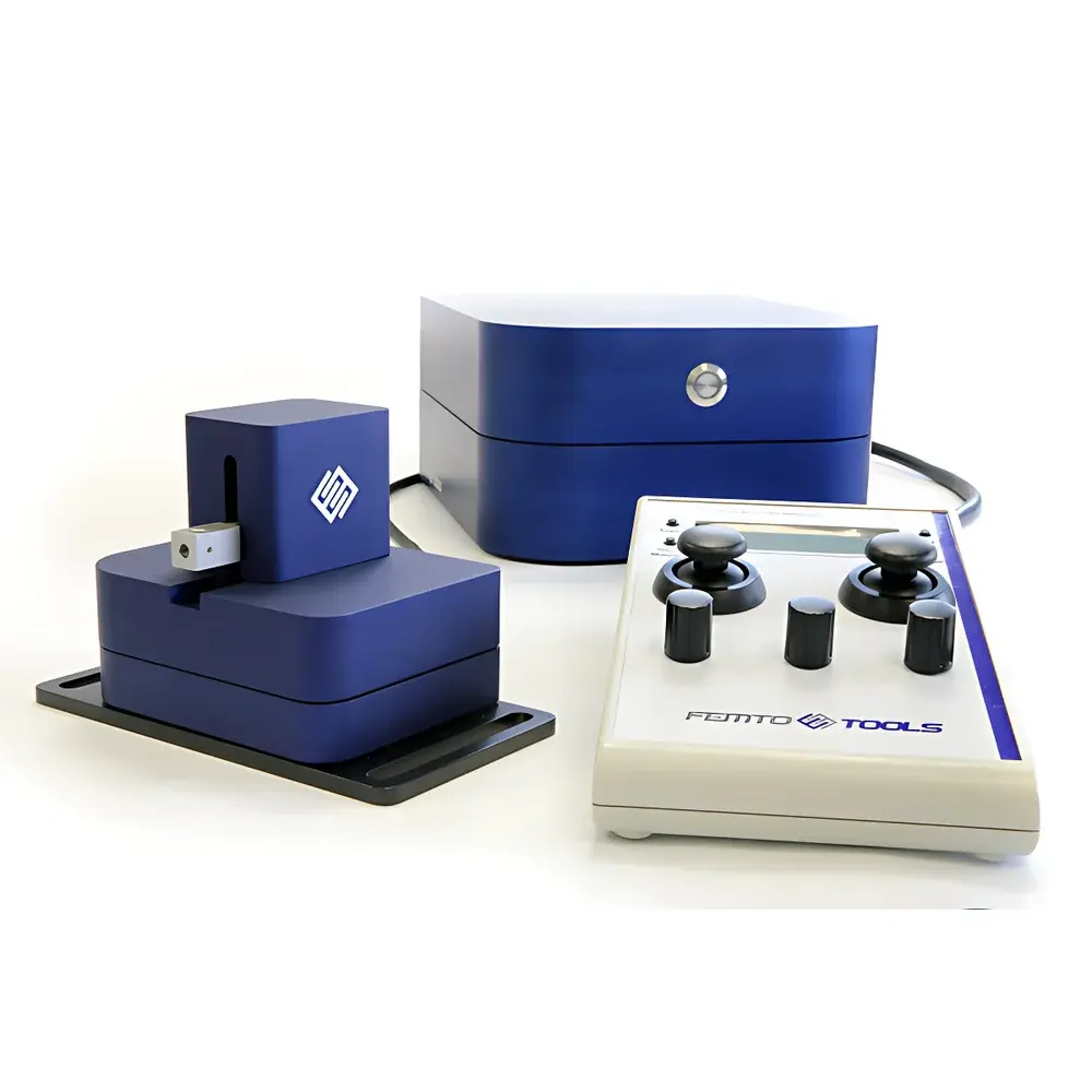
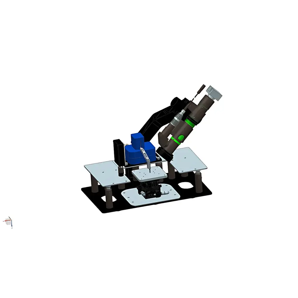
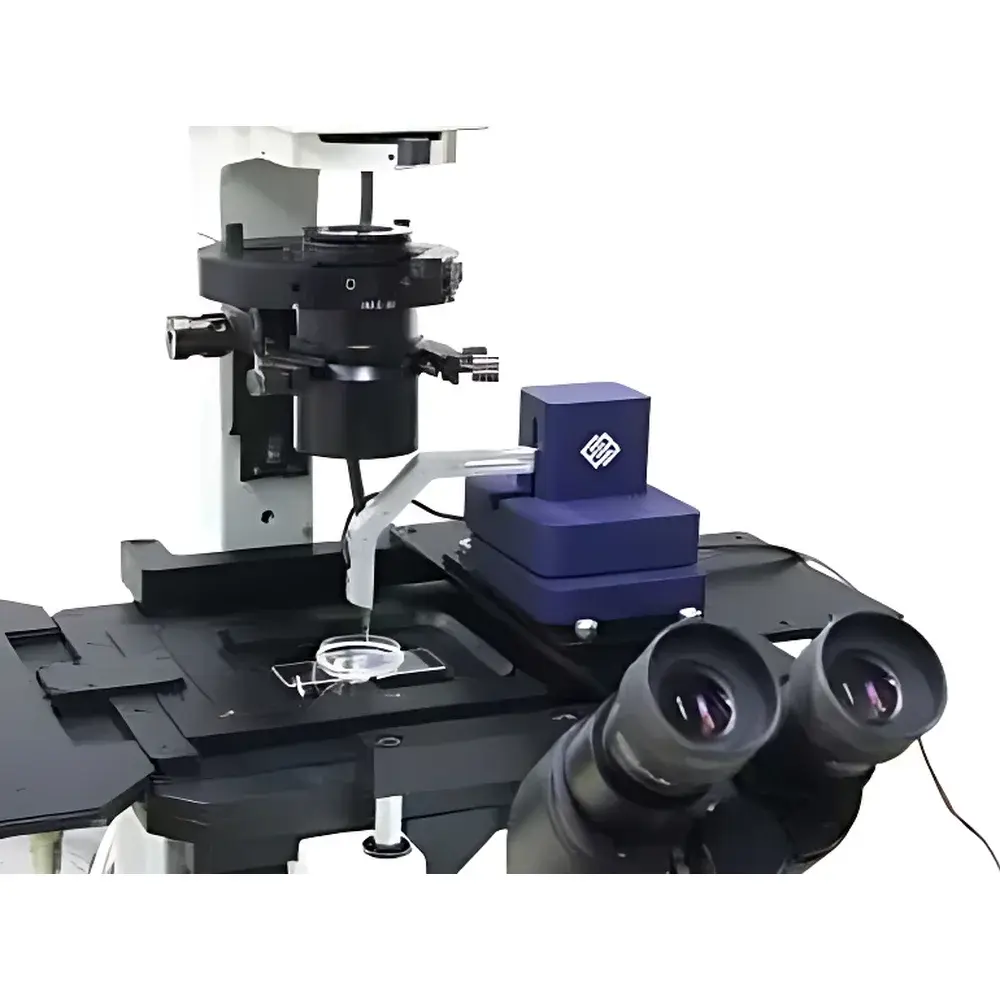
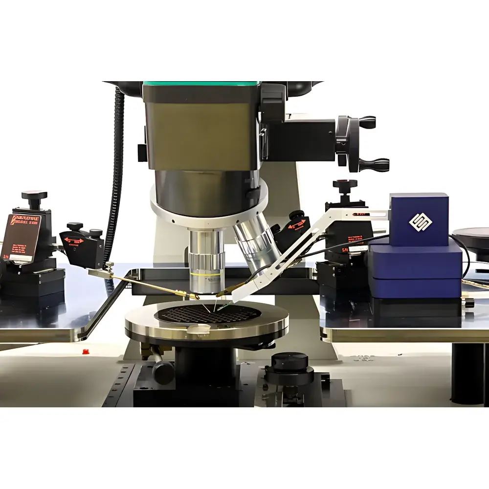
The FemtoTools FT-RS, FT-FS, FT-S, FT-G, and FT-UMS1000 series constitute a modular, high-precision nanomechanical testing and micromanipulation platform engineered for in situ quantitative mechanical characterization at the micro- and nanoscale. Built upon piezoresistive microelectromechanical systems (MEMS) force sensing technology, these instruments operate on the principle of direct force–displacement transduction—eliminating reliance on optical levers or capacitive feedback loops. This architecture enables real-time, closed-loop control with sub-nanometer displacement resolution and nano-Newton force sensitivity across dynamic loading regimes from static indentation to oscillatory testing (1 Hz – 8 kHz). Designed for integration within optical microscopes, probe stations, and scanning electron microscopes (SEM), the system supports fully visualized, multi-angle mechanical interrogation—including oblique and cross-sectional observation via optional motorized 0–180° rotating microscope stages (3 µm optical resolution, high-sensitivity CCD imaging). All platforms are developed and validated by FemtoTools AG, a Swiss spin-off of ETH Zurich’s Institute of Robotics and Intelligent Systems (IRIS), under the scientific leadership of Prof. Bradley Nelson.
Key Features
- Piezoresistive MEMS-based force sensors delivering calibrated force measurement from 5 nN to 10 mN with ≤1 nN resolution and linearity better than ±0.5% FS
- Active displacement control with 5 nm closed-loop resolution over ±100 µm range, enabling precise depth-sensing nanoindentation and controlled scratch profiling
- Integrated high-bandwidth actuation (up to 8 kHz) supporting dynamic mechanical analysis (DMA), creep/recovery, and fatigue testing protocols
- Modular probe head design compatible with interchangeable indenter geometries: Berkovich, cube-corner, spherical (1–50 µm radius), flat punch, and custom microfabricated tips
- In situ multimodal visualization: synchronized force–displacement–image acquisition with optional tilt-rotate microscope stage (0–180°), motorized Z-focus, and low-drift thermal management
- Vibration-isolated, compact benchtop form factor (<400 mm × 300 mm footprint); designed for cleanroom-compatible operation and electromagnetic compatibility (EMC Class B)
Sample Compatibility & Compliance
The FemtoTools platform accommodates a broad spectrum of solid-state materials—including thin films (SiO₂, SiNₓ, DLC), metallic coatings (Au, Ti, Ni), polymer membranes (PDMS, PMMA), biological specimens (cells, collagen fibrils, hydrogels), and MEMS/NEMS devices—without requiring conductive coating or vacuum preconditioning. Sample mounting is flexible: standard holders accept wafers up to 100 mm diameter; custom fixtures support irregular geometries and fragile substrates. The system complies with ISO 14577 (metallic and non-metallic coatings—nanoindentation), ASTM E2546 (standard guide for instrumented indentation testing), and supports audit-ready data generation aligned with GLP and GMP documentation requirements. Full traceability—including sensor calibration certificates (NIST-traceable reference standards), environmental logs (temperature, humidity), and operator metadata—is embedded in raw data export.
Software & Data Management
FemtoTools Control Suite v4.x provides deterministic real-time control (sub-millisecond loop timing), scriptable test sequencing (Python API), and synchronized multimodal data acquisition. Each experiment generates timestamped, HDF5-formatted datasets containing force, displacement, video frame triggers, and environmental parameters—ensuring FAIR (Findable, Accessible, Interoperable, Reusable) data principles. The software includes built-in modules for Oliver–Pharr analysis, pile-up/sink-in correction, modulus mapping, and statistical uncertainty quantification (Monte Carlo propagation). Export options include CSV, MATLAB .mat, and MTEX-compatible formats. For regulated environments, optional 21 CFR Part 11 compliance packages provide electronic signatures, role-based access control, and immutable audit trails with SHA-256 hashing of all raw and processed data.
Applications
- Quantitative nanomechanical mapping of interfacial adhesion, interlayer shear strength, and residual stress in multilayer semiconductor stacks
- In situ mechanical stimulation and force spectroscopy of single cells and extracellular matrix components under physiological buffer conditions
- Scratch resistance evaluation of protective coatings (e.g., anti-fingerprint layers, AR films) with simultaneous acoustic emission monitoring
- Micromanipulation-assisted device assembly: pick-and-place of microstructures (0–100 µm), nanowire alignment, and MEMS release testing
- Dynamic viscoelastic characterization of soft biomaterials using frequency-sweep nano-DMA, with storage/loss modulus extraction at sub-µm penetration depths
- Correlative nanomechanics–microscopy: combining SEM/EDS imaging with localized indentation to link composition gradients to mechanical heterogeneity
FAQ
What types of indenters are supported?
Standard configurations include Berkovich, cube-corner, spherical (1–50 µm radius), and flat-punch tips. Custom MEMS-fabricated tips (e.g., wedge, pyramidal, or bio-inspired geometries) can be integrated upon request.
Can the system operate inside an SEM chamber?
Yes—the FT-S and FT-G models are specifically engineered for ultra-high-vacuum SEM compatibility (≤10⁻⁶ mbar), featuring non-magnetic materials, low-outgassing cabling, and differential pumping interfaces.
Is thermal drift compensation automated?
Thermal drift is actively monitored via on-sensor temperature feedback; drift rates <0.1 nm/s are achieved under ambient temperature stability ±0.5 °C. Optional active thermal enclosure (±0.1 °C) further reduces long-term drift.
How is force calibration performed?
Calibration follows ISO 14577 Annex B using NIST-traceable reference cantilevers and electrostatic actuation verification. Certificate of calibration is provided with each sensor replacement.
Does the software support automated grid indentation?
Yes—grid mode allows user-defined x-y arrays (up to 1000×1000 points) with programmable dwell times, load ramps, and real-time property mapping (hardness, modulus, creep).


