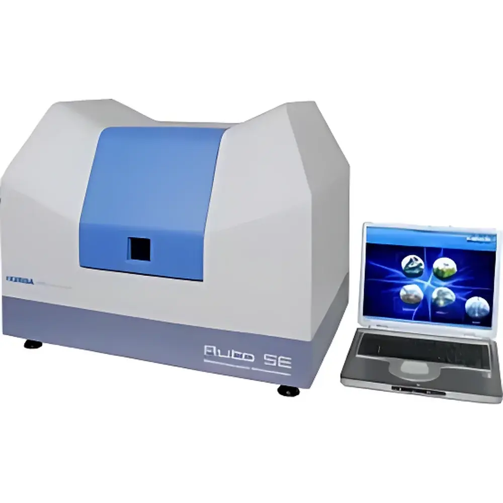
HORIBA Jobin Yvon Auto SE Automated Spectroscopic Ellipsometer
| Brand | HORIBA |
|---|---|
| Origin | France |
| Model | Auto SE |
| Spectral Range | 450–1000 nm |
| Incident Angle | 70° |
| Sample Stage | Motorized XYZ Translation (200 mm × 200 mm travel, Z-height > 35 mm) |
| Detection | CCD-based Full-Spectrum Acquisition |
| Optical Architecture | Liquid-Crystal Variable Retarder (LCVR) Modulation, No Moving Parts in Measurement Path |
| Spot Visualization | Integrated Real-Time Imaging System |
| Compliance | Designed for ISO/IEC 17025-aligned QC environments, supports audit-ready data logging per GLP/GMP principles |
Overview
The HORIBA Jobin Yvon Auto SE is a fully automated spectroscopic ellipsometer engineered for high-throughput, non-destructive thin-film characterization in industrial process control and R&D laboratories. It operates on the fundamental principle of spectroscopic ellipsometry—measuring the change in polarization state of light reflected from a sample surface across a broad spectral range (450–1000 nm). By analyzing the amplitude ratio (Ψ) and phase difference (Δ) between p- and s-polarized components, the system quantifies film thickness, optical constants (n, k), and interfacial structure with sub-nanometer sensitivity for single- and multi-layer stacks. Its fixed 70° angle of incidence provides optimal sensitivity for common dielectric and semiconductor films (e.g., SiO₂, SiNₓ, ITO, photoresists), while eliminating angular alignment complexity and enabling robust integration into production line workflows.
Key Features
- True one-button operation: Initiation of measurement, model fitting, and report generation is executed via a single GUI command—no manual alignment or parameter tuning required.
- LCVR-based optical modulation: Replaces traditional rotating compensators with solid-state liquid-crystal variable retarders, ensuring long-term stability, zero mechanical wear, and immunity to vibration-induced drift.
- CCD spectrometer detection: Captures the full spectrum (450–1000 nm) in a single acquisition cycle, delivering high signal-to-noise ratio and enabling rapid (< 5 s typical) measurement repeatability.
- Real-time spot visualization: Integrated high-resolution imaging optics allow operators to precisely position the measurement spot on patterned wafers, defects, or heterogeneous surfaces—critical for inline metrology and failure analysis.
- Motorized XYZ stage: Supports automated mapping of 200 mm × 200 mm substrates with programmable grid patterns; Z-axis travel exceeds 35 mm to accommodate thick carriers, cassettes, or fixtures.
- Sealed sample chamber: Minimizes environmental contamination and thermal drift, enhancing measurement reproducibility across shifts and ambient conditions.
Sample Compatibility & Compliance
The Auto SE accommodates rigid planar substrates up to 200 mm × 200 mm, including silicon wafers, glass panels, metal foils, and ceramic tiles. Its non-contact, non-destructive methodology is compatible with temperature-sensitive layers (e.g., organic semiconductors, polymer resists) and fragile nanostructures. The instrument conforms to foundational metrological requirements for industrial QA/QC: it supports traceable calibration using NIST-traceable reference standards, enables user-defined uncertainty budgets, and logs all acquisition parameters—including lamp intensity, stage coordinates, and environmental timestamps—for compliance with ISO 9001, ISO/IEC 17025, and internal GLP protocols. While not FDA-certified as a medical device, its data integrity architecture aligns with 21 CFR Part 11 expectations for electronic records and signatures when deployed with validated software configurations.
Software & Data Management
Equipped with HORIBA’s DeltaPsi² software suite, the Auto SE provides intuitive workflow management—from quick-start templates for routine film types (SiO₂/Si, SiNₓ/Si, etc.) to advanced modeling of graded interfaces, roughness layers, and anisotropic materials. All raw Ψ(λ) and Δ(λ) spectra, fitted models, and residual plots are stored in vendor-neutral HDF5 format. The software includes built-in statistical process control (SPC) dashboards, batch reporting tools, and API access for integration with MES or factory automation systems (e.g., SECS/GEM). Audit trails record operator ID, timestamp, parameter edits, and version-controlled model definitions—ensuring full traceability during regulatory inspections.
Applications
- Front-end semiconductor manufacturing: Thickness and uniformity monitoring of gate oxides, anti-reflective coatings, and hard masks on 200 mm wafers.
- Flat-panel display production: In-line verification of ITO, Mo, and Al alloy films on large-area glass substrates.
- Photovoltaic R&D: Characterization of CIGS absorber layers, perovskite stack interfaces, and transparent conductive oxides.
- MEMS and packaging: Quantification of passivation layer integrity and stress-induced birefringence in encapsulated devices.
- Academic thin-film physics: Investigation of plasmonic nanostructures, 2D material heterostructures, and stimuli-responsive polymer films.
FAQ
What film thickness range can the Auto SE measure?
The system is optimized for films from ~0.5 nm to ~5 µm, depending on material optical constants and layer structure. Sub-monolayer sensitivity is achievable for high-contrast interfaces (e.g., SiO₂ on Si).
Is vacuum or nitrogen purging required for UV extension?
No—the 450–1000 nm range operates reliably in ambient air; no purge gas or vacuum chamber is needed.
Can the Auto SE be integrated into a cleanroom environment?
Yes—its sealed chamber, low particulate emission design, and ESD-safe construction meet Class 1000 cleanroom compatibility standards.
Does the software support custom optical models?
Yes—DeltaPsi² allows user-defined dispersion models (e.g., Tauc-Lorentz, Cody-Lorentz), multi-layer stacks with gradient layers, and effective medium approximations for nanocomposites.
How is calibration maintained over time?
The system employs a dual-reference approach: factory-calibrated LCVR response curves plus optional in-situ validation using certified Si/SiO₂ reference wafers at user-defined intervals.


