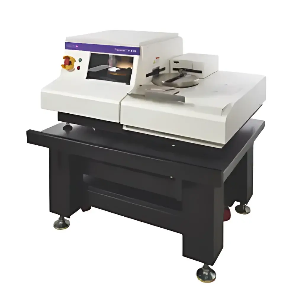
KLA P-170 Stylus Profilometer
| Brand | KLA |
|---|---|
| Origin | Malaysia |
| Manufacturer Type | Authorized Distributor |
| Product Origin | Imported |
| Model | P-170 |
| Product Category | Contact Stylus Profilometer / Surface Roughness Tester |
| Operating Principle | Stylus-based Contact Profilometry |
Overview
The KLA P-170 Stylus Profilometer is a production-grade, automated surface metrology system engineered for high-reproducibility 2D and 3D topographic characterization in semiconductor fabrication, compound semiconductor manufacturing, MEMS development, and advanced optoelectronics R&D. Based on proven contact profilometry principles—where a diamond-tipped stylus physically traverses the sample surface while measuring vertical displacement via linear variable differential transformer (LVDT) or capacitive transduction—the P-170 delivers traceable, NIST-compatible measurements of step height, surface roughness (Ra, Rq, Rz), waviness, bow, warp, and thin-film stress. Its mechanical architecture integrates the field-proven HRP®-260 robotic platform with the high-precision motion control and metrology engine of the KLA P-17 desktop system, enabling robust, repeatable performance across 24/7 fab environments. With a continuous scan range of up to 200 mm without image stitching and sub-nanometer vertical resolution, the P-170 bridges the gap between lab-grade accuracy and high-throughput inline process control.
Key Features
- Stylus-based contact measurement with UltraLite® sensor technology and active micro-force control (0.03–50 mg), minimizing surface deformation on soft films and delicate substrates
- Integrated high-stability scanning stage with ultra-flat Z-axis motion (<±2 nm flatness over 200 mm travel), enabling accurate large-area mapping without stitching artifacts
- 5 MP full-color coaxial and side-view optical imaging system with motorized optical zoom, supporting rapid feature identification, alignment, and ROI selection
- Advanced arc correction algorithm compensating for stylus path curvature—critical for maintaining nanoscale accuracy on curved or warped wafers
- Automated wafer handling with SECS/GEM-compliant robotic arm support for 75–200 mm opaque (e.g., Si, GaAs) and transparent (e.g., sapphire, quartz) substrates
- Graphical pattern recognition engine enabling auto-sequence execution, fiducial-based alignment, and feature-driven measurement scripting
- Vacuum chuck stage standard; optional stress stage with three-point kinematic mounting for precise bow/warp and film stress analysis per ASTM F390 and ISO 14644-1
Sample Compatibility & Compliance
The P-170 accommodates rigid and semi-rigid planar substrates from 75 mm to 200 mm in diameter, including silicon, gallium arsenide, silicon carbide, sapphire, fused silica, and glass wafers. Its vacuum stage supports both conductive and insulating surfaces, while optional ionizers mitigate electrostatic charge buildup during scanning of dielectric layers. The system complies with SEMI E10 (Specification for Definition and Measurement of Equipment Reliability, Maintainability, and Availability), SEMI E30 (SECS/GEM Communications Standard), and supports audit-ready data integrity per FDA 21 CFR Part 11 when configured with KLA’s certified software package. All measurement algorithms—including Gaussian filtering, polynomial leveling, and ISO 4287–4288–4289–11562 compliant roughness parameter extraction—are fully documented and validated under GLP-aligned internal procedures.
Software & Data Management
The P-170 operates on KLA’s industry-standard WinPro™ software platform, featuring an intuitive, icon-driven interface optimized for operator efficiency and minimal training overhead. Measurement workflows are programmable via drag-and-drop sequencing, with built-in libraries for common semiconductor structures (e.g., photoresist stacks, metal interconnects, etch stop layers). Raw profile data is stored in vendor-neutral ASCII and HDF5 formats; all analysis parameters—including filter cutoffs, reference plane definitions, and statistical reporting thresholds—are embedded as metadata. Audit trails record user actions, method changes, calibration events, and instrument configuration states with time-stamped, immutable logs. Integration with factory MES systems is supported through native OPC UA and REST API endpoints for real-time SPC dashboarding and automated yield correlation.
Applications
- Step Height Metrology: Quantification of lithographic resist thickness, etch depth, CMP removal, and deposition uniformity across full wafers (2D line scans and 3D surface maps)
- Roughness & Texture Analysis: Evaluation of surface finish post-CMP, plasma etching, or thermal oxidation per ISO 25178 and ASTM E2382
- Wafer Geometry: Full-diameter bow, warp, TTV (Total Thickness Variation), and site-specific flatness assessment per SEMI MF-1530
- Thin-Film Stress: Derivation of biaxial stress from curvature measurements using Stoney’s equation, calibrated against reference standards
- Defect Topography: High-resolution 3D reconstruction of particle-induced scratches, pits, and residue features for root-cause failure analysis
FAQ
What is the minimum measurable step height and vertical resolution?
The P-170 achieves sub-nanometer vertical resolution (typically <0.1 nm RMS noise floor) and reliably measures steps down to 1 nm in controlled environments, subject to probe radius, surface reflectivity, and environmental vibration isolation.
Can the system measure transparent substrates like sapphire or fused silica?
Yes—integrated top- and side-view optics with adjustable illumination enable precise autofocus and stylus positioning on both opaque and transparent materials without requiring conductive coatings.
Is the P-170 suitable for cleanroom deployment?
The system meets ISO Class 5 (Class 100) cleanroom compatibility requirements when installed with appropriate air filtration and anti-vibration mounts; full SEMI-compliant documentation packages are available upon request.
Does it support automated recipe transfer between tools?
Yes—measurement programs, calibration files, and analysis settings are fully portable across P-170 systems via encrypted project archives, ensuring consistent cross-tool metrology performance in multi-tool fabs.
What calibration standards are recommended for routine verification?
KLA recommends traceable step-height standards (e.g., NIST SRM 2160, VLSI Standards PS-1 series) and roughness standards (e.g., NIST SRM 1960, Taylor Hobson TG series), with annual calibration services available through KLA-certified service centers.