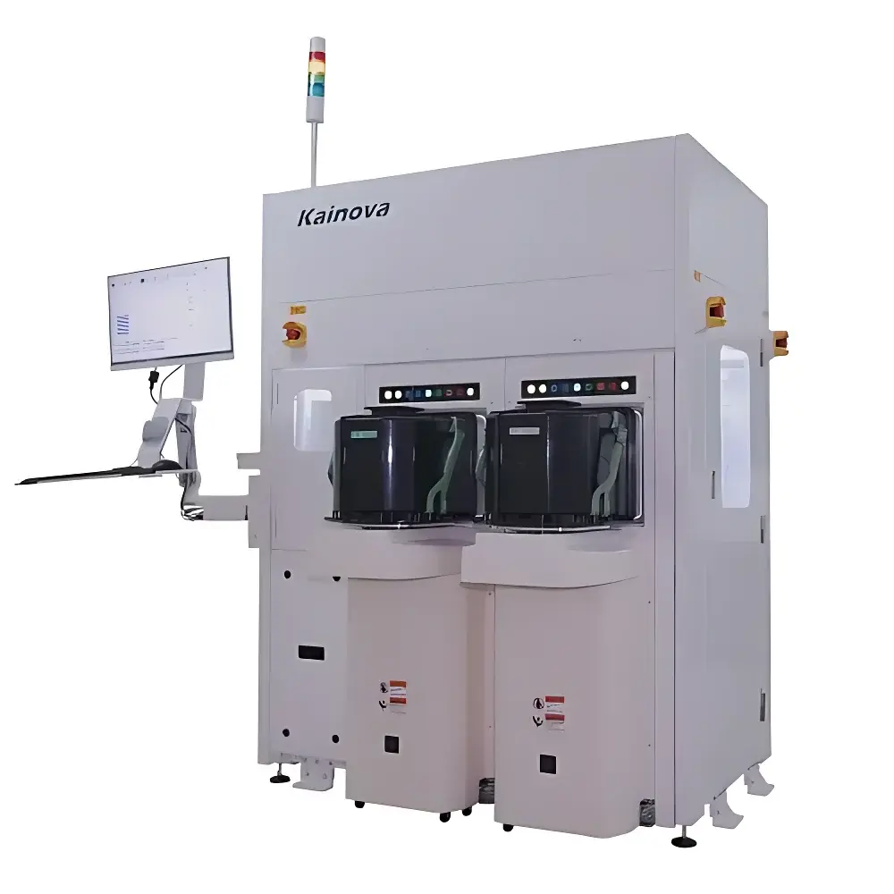
Kainova Tech KAR-211 Wafer Handling Automation System
| Brand | Kainova |
|---|---|
| Origin | Taiwan |
| Manufacturer Type | Authorized Distributor |
| Product Category | Domestic (Taiwan-made) |
| Model | KAR-211 |
| Pricing | Upon Request |
| Load Ports | 2–8 configurable |
| Motion Control | 5-axis dual-end-effector robot |
| Wafer Compatibility | 200 mm (8″), 300 mm (12″), and thinned wafers (≤725 µm) |
| Dual-Side Wafer ID Reading | OCR + barcode (SEMI P17 compliant) |
| Interface Standards | SECS/GEM v2.0, SEMI E84 OHT Handshake Protocol |
| Cleanroom Certification | ISO Class 3 (FS-209E Class 1) |
| Throughput | ≥700 WPH |
| Positioning Accuracy | ±0.05 mm |
| Airflow Design | FFU-controlled laminar downflow with CFD-validated uniform velocity profile (0.45 ±0.05 m/s) |
| Safety & Compliance | SEMI S2-0215 Certified |
Overview
The Kainova Tech KAR-211 Wafer Handling Automation System is an integrated front-end material handling platform engineered for high-precision, high-throughput wafer transport in advanced semiconductor fabrication environments. Based on a rigid mechanical architecture and real-time motion control architecture, the system implements deterministic robotic handling using a 5-axis dual-gripper robot — eliminating the need for external track-based conveyance while maintaining sub-50 µm repeatability across full wafer transfer cycles. Its core function is intelligent wafer routing: receiving wafers via configurable load ports (2–8 units), executing recipe-driven sorting, batching, merging, or destination-specific placement into FOUPs, FOSBs, or process tools — all synchronized via SECS/GEM messaging. The system operates within ISO Class 3 cleanroom conditions (FS-209E Class 1), supported by nitrogen-purged load ports, micro-positive pressure control, and a CFD-optimized laminar airflow system ensuring particle-free wafer transit.
Key Features
- Configurable modular load port architecture supporting 2–8 ports with independent N₂ purge and vacuum integrity monitoring.
- Dual-end-effector 5-axis robot with dynamic path optimization, enabling simultaneous pick-and-place operations without mechanical interference.
- Integrated dual-side wafer identification subsystem compliant with SEMI P17 standards — combining high-speed OCR and barcode decoding for unambiguous wafer traceability.
- Real-time environmental control: programmable FFU speed, chamber pressure differential (≥15 Pa micro-positive), and temperature/humidity monitoring (±0.5°C / ±3% RH).
- Full SEMI E84-compliant overhead hoist transport (OHT) handshake protocol implementation for seamless integration with factory automation systems.
- SEMI S2-0215 certified mechanical and electrical safety design, including emergency stop zoning, light curtain interlocks, and torque-limited motion profiles.
Sample Compatibility & Compliance
The KAR-211 accommodates standard semiconductor substrates including 200 mm and 300 mm silicon wafers, as well as mechanically thinned wafers down to 50 µm thickness. It supports both bare and film-coated wafers, with edge exclusion handling compliant with SEMI M1–0216. All internal surfaces are electropolished stainless steel (ASTM A967) with low-outgassing elastomers meeting SEMI F21 requirements. The system is fully compliant with ISO 14644-1 Class 3 (equivalent to FS-209E Class 1), validated per IEST-RP-CC006.2. Electrical safety follows UL 61010-1 and EN 61000-6-2/6-4. Documentation includes full traceable calibration records, FAT/SAT reports, and SEMI E10-compliant reliability test summaries.
Software & Data Management
The embedded control software runs on a real-time Linux OS with deterministic scheduling and dual-redundant EtherCAT communication. Recipe management supports hierarchical configuration (tool-level → lot-level → wafer-level), with version-controlled parameter sets stored in encrypted SQLite databases. All wafer movements are logged with timestamps, source/destination IDs, gripper status, and environmental telemetry — generating audit-ready CSV and XML logs compliant with FDA 21 CFR Part 11 requirements (electronic signatures, audit trails, data immutability). Integration with MES is achieved via standard GEM300 interface; historical logs can be exported to SQL Server or Oracle via ODBC drivers. Remote diagnostics support TLS 1.2-secured SSH and VNC sessions with role-based access control (RBAC).
Applications
The KAR-211 serves as a critical node in 300 mm advanced packaging lines, EUV lithography clusters, and compound semiconductor manufacturing where wafer-level metrology and defect review tools require uninterrupted, contamination-controlled input. Typical deployment scenarios include: (1) pre-litho wafer sorting prior to mask alignment; (2) post-etch/post-CMP buffer staging before optical inspection; (3) automated rework loop integration with defect mapping systems (e.g., KMM-332); (4) hybrid inline/out-of-line configurations interfacing with cluster tools and standalone metrology stations. Its dual-gripper architecture enables concurrent loading/unloading of adjacent process modules, reducing tool idle time and increasing overall equipment effectiveness (OEE).
FAQ
Does the KAR-211 support thin-wafer handling below 100 µm?
Yes — the robot end-effectors feature adaptive vacuum compensation and edge-sensing feedback loops calibrated for wafers as thin as 50 µm, with verified no-slip performance under full acceleration profiles.
Can the system be retrofitted into existing 200 mm fabs?
Yes — footprint-optimized variants are available with reduced height and modular load port mounting kits compatible with legacy fab floor layouts and ceiling grid constraints.
Is the SECS/GEM interface certified by SEMI?
Yes — the GEM300 stack has passed SEMI E30/E37/E40 conformance testing and is registered in the SEMI Interoperability Registry (SIR) under certificate #GEM-2023-KAI-0884.
What maintenance intervals are recommended for the robot drive system?
Linear guide rails and harmonic drives require lubrication every 2,000 operating hours; encoder calibration and gripper vacuum verification are scheduled every 500 hours per SEMI E10 guidelines.
How is particle generation controlled during wafer transfer?
All moving components utilize brushless DC motors with shielded cabling; wafer contact surfaces employ static-dissipative PEEK composites (10⁶–10⁹ Ω/sq); airborne molecular contamination (AMC) is monitored continuously via integrated PID sensors with alarm thresholds aligned to SEMI F21 Annex B.


