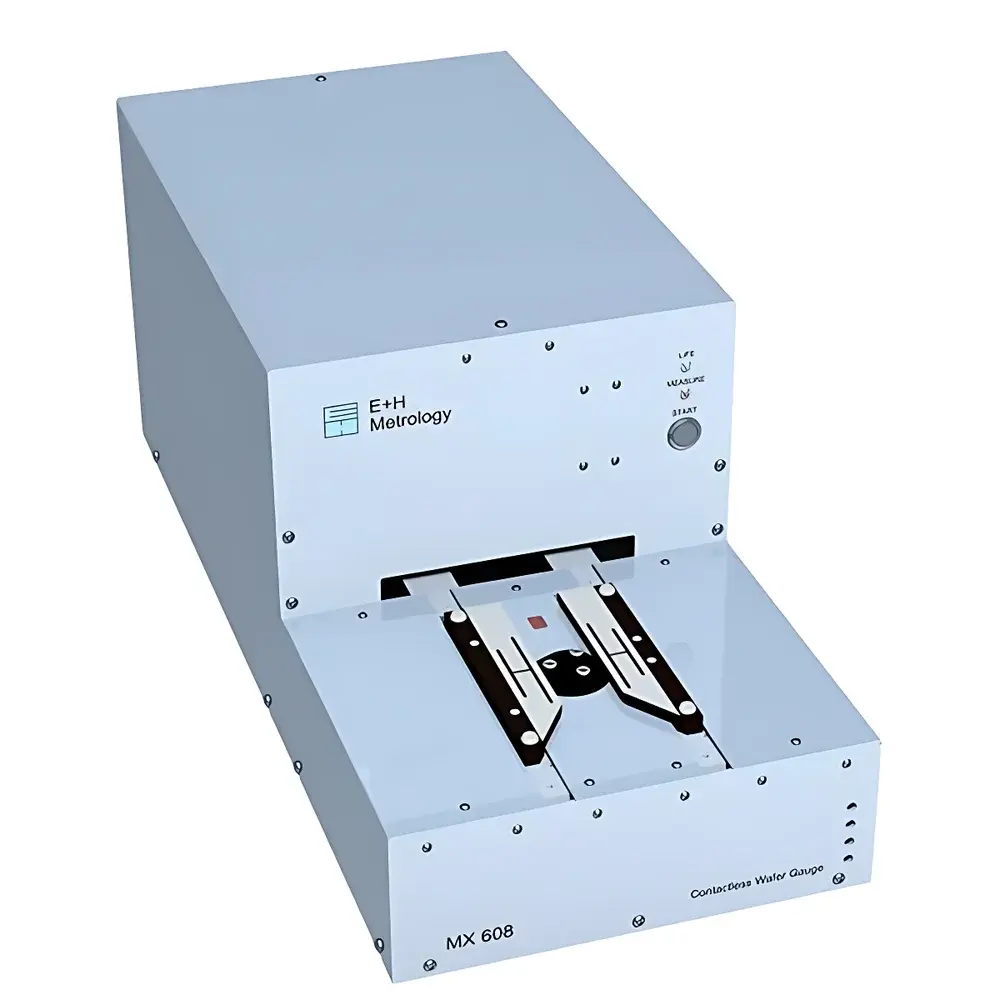
E+H Metrology MX608 Non-Contact Wafer Thickness & Resistivity Metrology System
| Brand | E+H Metrology |
|---|---|
| Origin | Germany |
| Model | MX 608 |
| Wafer Sizes Supported | 4", 5", 6", 8" |
| Thickness Range | 300–800 µm (standard 500–800 µm) |
| Max. Warp | 100 µm |
| Resistivity Range | 0.001–200 Ω·cm |
| Thickness Accuracy | ±0.3 µm |
| TTV Accuracy | ±0.1 µm |
| Thickness Resolution | ±0.05 µm |
| Resistivity Accuracy | ±1% (0.001–30 Ω·cm), ±2% (30–100 Ω·cm), ±5% (100–200 Ω·cm) |
| Measurement Time | 7 s (single-point center), 10 s (full radial scan, 180 points on 8″ wafer), ~3 min (18 angular scans × 180 points = 3240-point full mapping) |
Overview
The E+H Metrology MX608 is a high-precision, non-contact metrology platform engineered for simultaneous thickness, total thickness variation (TTV), and bulk resistivity characterization of semiconductor wafers. It employs eddy-current and capacitive sensing principles—fully decoupled and independently calibrated—to deliver traceable, repeatable measurements without physical contact, surface preparation, or electrical probing. Designed specifically for front-end process control in silicon, silicon carbide (SiC), gallium nitride (GaN), and other conductive or semi-insulating substrates, the MX608 supports inline integration into cleanroom environments and meets the dimensional stability and thermal drift requirements of advanced node fabrication (≤28 nm). Its modular sensor architecture allows configurable deployment for both single-point verification and full-wafer mapping, enabling correlation between structural uniformity (thickness/TTV) and electrical homogeneity (resistivity distribution)—a critical capability for epitaxial layer validation, donor/acceptor concentration profiling, and post-anneal uniformity assessment.
Key Features
- True non-contact operation: No vacuum chucking, no probe contact, no surface contamination risk—ideal for fragile, ultra-thin, or patterned wafers.
- Dual-sensor fusion: Integrated eddy-current (for resistivity) and capacitive (for thickness/TTV) transducers with real-time cross-compensation for temperature-induced drift and substrate dielectric variability.
- Full-wafer mapping capability: Programmable scanning patterns—including radial, spiral, and grid-based acquisition—with up to 3240 measurement points per 8″ wafer, fully compliant with SEMI MF1530 and ASTM F39 standards for spatial data reporting.
- Automated edge exclusion and notch/flat detection: On-the-fly recognition of wafer geometry using optical edge sensors; configurable exclusion zones (e.g., 2 mm from edge) ensure metrological integrity at critical process margins.
- Robust thermal management: Active temperature stabilization of sensor head and stage (±0.1 °C) minimizes thermal expansion artifacts, supporting long-term measurement repeatability (GR&R < 1.2% at 3σ over 24 h).
- Modular calibration architecture: NIST-traceable reference wafers for thickness (certified SiO₂-on-Si standards) and resistivity (doped Si calibration sets) enable on-site verification and periodic requalification per ISO/IEC 17025 requirements.
Sample Compatibility & Compliance
The MX608 accommodates bare and processed wafers across 4″, 5″, 6″, and 8″ diameters, including polished, epitaxially grown, oxidized, and bonded substrates. It supports conductive materials (Si, SiC, GaN, Ge) as well as semi-insulating substrates (e.g., AlN, sapphire with conductive backside metallization) via adaptive signal conditioning. All measurement protocols align with industry-standard specifications: SEMI MF1530 (wafer thickness measurement), ASTM F39 (resistivity of silicon wafers), and ISO 14644-1 Class 5 cleanroom compatibility. The system’s mechanical design conforms to SEMI S2/S8 safety guidelines, and its software architecture supports audit-ready data handling in accordance with FDA 21 CFR Part 11 and EU Annex 11 for regulated semiconductor manufacturing environments.
Software & Data Management
The MX608 operates under E+H’s proprietary MetroSuite™ v4.2 software, a Windows-based application certified for GMP/GLP workflows. It provides real-time visualization of thickness and resistivity maps, statistical process control (SPC) charting (X-bar/R, Cpk/Ppk), and automated pass/fail evaluation against user-defined specification limits (e.g., TTV ≤ 0.5 µm, resistivity uniformity ≤ ±3%). Raw data is stored in HDF5 format with embedded metadata (timestamp, operator ID, calibration status, environmental conditions), ensuring full traceability. Export options include CSV, XML (SEMI E126-compliant), and direct OPC UA integration for MES/SCADA connectivity. Audit trails record all parameter changes, measurement executions, and calibration events—with immutable timestamps and digital signature support.
Applications
- Front-end process monitoring: In-line verification of CZ/FZ crystal ingot slicing, wafer lapping/polishing, and chemical-mechanical planarization (CMP) uniformity.
- Epitaxial layer qualification: Correlation of epi-layer thickness (via capacitance offset) and carrier concentration (via resistivity gradient) to detect dopant segregation or interfacial defects.
- Compound semiconductor R&D: Characterization of SiC and GaN substrates for power device fabrication, where thickness uniformity directly impacts breakdown voltage consistency.
- Outgoing quality assurance: Final wafer release testing per customer-specific AQL plans, with automated report generation compliant with IATF 16949 and ISO 9001 documentation requirements.
- Process development support: Statistical analysis of tool-to-tool matching (e.g., between CMP tools or annealing furnaces) using multi-wafer, multi-lot datasets.
FAQ
Does the MX608 require electrical contact or backside metallization for resistivity measurement?
No. The system uses low-frequency eddy-current excitation (1–10 MHz) that penetrates insulating layers and induces measurable currents in the conductive bulk—enabling accurate resistivity determination even on oxide-coated or unmetallized wafers.
Can the MX608 measure patterned or device wafers?
Yes. Its non-contact approach and sub-millimeter spot size (capacitive: Ø0.8 mm; eddy-current: Ø1.2 mm) allow reliable measurement on partially processed wafers, provided the local topography does not exceed ±5 µm step height within the sensor footprint.
How is system accuracy maintained over time?
Through scheduled recalibration using NIST-traceable reference wafers, combined with daily verification runs and automated thermal drift compensation algorithms embedded in the firmware.
Is the MX608 compatible with automated material handling systems (AMHS)?
Yes. It supports SECS/GEM communication protocol and offers optional robotic interface modules (SMIF/FOUP load ports) for integration into cluster tools and factory automation infrastructures.
What training and service support is available?
E+H Metrology provides on-site installation qualification (IQ), operational qualification (OQ), and comprehensive operator certification programs. Global service coverage includes remote diagnostics, preventive maintenance contracts, and spare sensor head exchange within 72 hours under platinum support agreements.


