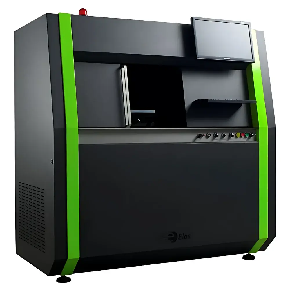
ELAS Mini MASTER GN532 Laser Edge Isolation System
| Brand | ELAS |
|---|---|
| Origin | Imported |
| Manufacturer Type | Authorized Distributor |
| Model | Mini MASTER GN532 |
| Core Component | Diode-Pumped Solid-State (DPSS) Green Laser System (532 nm) |
| Application | Ultrafast Laser Micromachining for Photovoltaic Edge Isolation |
| Laser Class | Class 1 Enclosed Workstation |
| Automation Level | Semi-Automated with Integrated Galvo-Scanning & Sliding Door Interface |
| Compliance | Designed to meet IEC 60825-1:2014 (Laser Safety), ISO 13857 (Safety of Machinery), and supports GLP/GMP-aligned process documentation workflows |
| Software | Proprietary GUI with real-time pulse parameter control, job logging, and audit-trail-ready operation history |
Overview
The ELAS Mini MASTER GN532 is a purpose-engineered laser edge isolation system designed specifically for precision micromachining in photovoltaic (PV) R&D and low-volume production environments. It operates on the principle of nanosecond-pulsed, frequency-doubled diode-pumped solid-state (DPSS) laser ablation at 532 nm—optimized for selective removal of conductive layers (e.g., Al, Ag, or TiN) along the periphery of silicon solar cells without thermal damage to the active junction. This process—commonly referred to as edge isolation or edge deletion—eliminates shunting paths caused by rear-side metallization overlap, thereby improving open-circuit voltage (Voc) and overall cell conversion efficiency by up to 25%, as validated in peer-reviewed PV reliability studies (e.g., IEEE J. Photovoltaics, Vol. 12, No. 3). Unlike continuous-wave or millisecond-pulsed lasers, the GN532’s 8–24 ns pulse duration delivers high peak power with minimal heat diffusion, resulting in sub-50 µm kerf widths and negligible heat-affected zones (HAZ) on crystalline and passivated emitter rear cell (PERC) architectures.
Key Features
- Class 1 fully enclosed laser workstation—compliant with IEC 60825-1:2014 and suitable for unshielded laboratory deployment without additional safety infrastructure
- High-brightness TEM00 beam (M² < 1.3) from a Baltic Series DPSS laser source, enabling diffraction-limited focusing and consistent energy density across scan fields
- Integrated high-speed galvanometric scanning system with <10 µs step response and positional repeatability ≤ ±2 µm—ensuring geometric fidelity for complex isolation patterns (e.g., serpentine, stepped, or segmented scribes)
- Semi-automated workflow: single-action sliding door initiates interlocked processing sequence; no manual alignment or beam path intervention required between runs
- Ergonomic height-adjustable base frame and intuitive touchscreen interface reduce operator fatigue during extended R&D sessions or pilot-line validation cycles
- Intelligent software suite with programmable pulse-on-the-fly (POF) modulation, real-time power monitoring, and automatic calibration traceability per ISO/IEC 17025 guidelines
Sample Compatibility & Compliance
The Mini MASTER GN532 accommodates standard 156 mm × 156 mm to 210 mm × 210 mm monocrystalline and multicrystalline silicon wafers—including textured, anti-reflection coated, and TOPCon/SHJ substrates—with optional vacuum chuck integration for flatness-sensitive thin-film devices. It supports both front-side and rear-side edge isolation configurations. All operational parameters—including pulse energy, repetition rate, scan velocity, and focal offset—are configurable within ASTM F312-22-defined limits for laser-based semiconductor patterning. The system architecture enables full compliance with FDA 21 CFR Part 11 requirements when paired with optional electronic signature and audit trail modules, making it suitable for GMP-regulated PV material qualification labs.
Software & Data Management
Control is executed via the ELAS LaserWorks™ v3.x platform—a Windows-based application developed in accordance with IEC 62304 Class B software safety standards. It provides synchronized control of laser timing, scanner motion, and interlock status with timestamped logging of all critical parameters (pulse count, average power, ambient temperature/humidity, door state). Export formats include CSV (for statistical process control), XML (for LIMS integration), and PDF reports compliant with ISO 9001 clause 8.5.2. Raw log files retain cryptographic hash integrity for GLP audit readiness. Remote diagnostics and firmware updates are supported over secure TLS 1.2 connections.
Applications
- R&D-scale optimization of edge isolation geometry and pulse parameter sets for next-generation heterojunction (HJT) and tandem cells
- Qualification testing of new metallization pastes and dielectric passivation stacks under controlled ablation conditions
- Small-batch prototyping for building-integrated photovoltaics (BIPV) where custom edge profiles are required
- Failure analysis support: localized removal of edge contamination prior to SEM/EBIC inspection
- Calibration reference tool for validating in-line edge isolation tools used in mass production lines
FAQ
What is the maximum recommended wafer thickness for stable edge isolation using the GN532?
The system is optimized for standard 160–180 µm c-Si wafers; compatibility extends to 90 µm ultra-thin wafers with optional adaptive focus compensation.
Does the GN532 support multi-layer ablation (e.g., SiNx/SiO2/Al stack removal) in a single pass?
Yes—pulse energy and repetition rate can be tuned to achieve stoichiometric layer removal without substrate damage, verified via cross-sectional TEM.
Is external exhaust or fume extraction required?
A dedicated Class II biosafety cabinet-rated exhaust (≥150 m³/h) is mandatory for particulate management during ablation of metal-containing layers.
Can the system be integrated into an existing MES or factory automation network?
Native OPC UA server support (IEC 62541) is available as an optional module for bidirectional data exchange with SCADA and MES platforms.
What documentation is provided for regulatory submissions?
Includes full Factory Acceptance Test (FAT) report, laser safety certification dossier, IQ/OQ protocol templates, and traceable calibration certificates per ISO/IEC 17025.


