Hitachi High-Tech FlexSEM 1000 II Desktop Scanning Electron Microscope
| Brand | Hitachi High-Tech |
|---|---|
| Origin | Japan |
| Manufacturer | Hitachi High-Technologies Corporation |
| Product Type | Imported Desktop SEM |
| Model | FlexSEM 1000 II |
| Electron Source | Tungsten Filament |
| Secondary Electron Resolution | 4.0 nm @ 20 kV (High Vacuum), 15.0 nm @ 1 kV (High Vacuum) |
| Backscattered Electron Resolution | 5.0 nm @ 20 kV (Low Vacuum) |
| Magnification Range | 6×–300,000× (Film Equivalent), 16×–800,000× (Display) |
| Accelerating Voltage | 0.3–20 kV |
| EDS Detector | 30 mm² Silicon Drift Detector (SDD), Nitrogen-free |
| Dimensions (Main Unit) | 450 mm (W) × 640 mm (D) |
| Power Interface | Standard IEC C13 Socket |
| System Architecture | Modular Main Unit + Detachable Power Supply Unit |
Overview
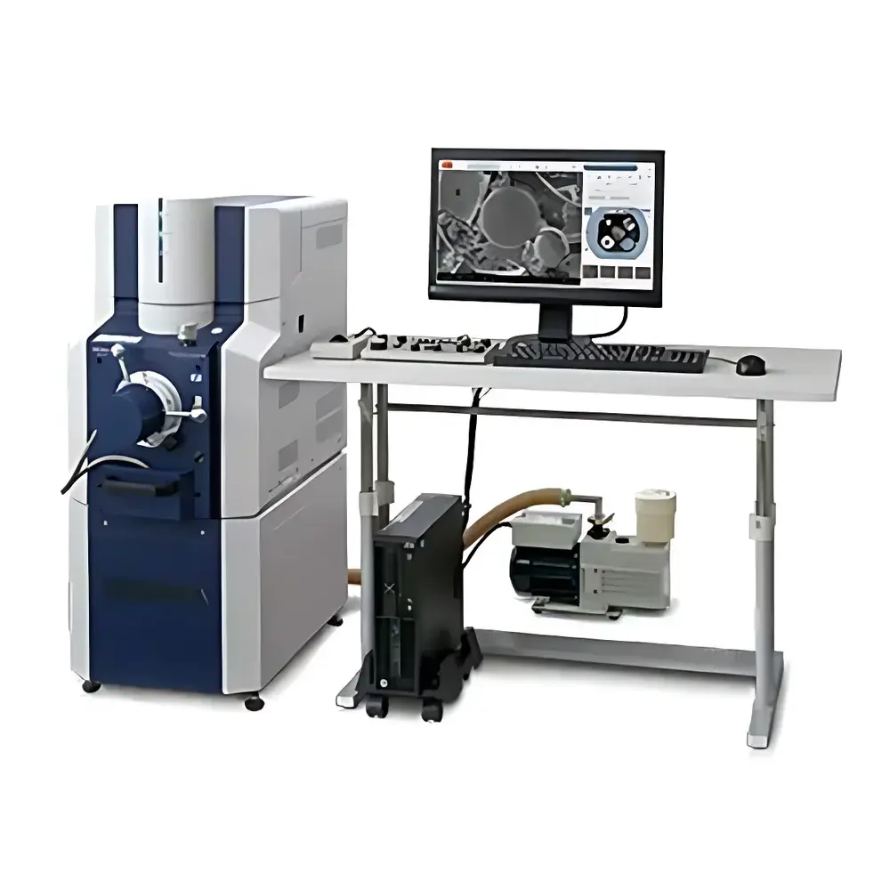
The Hitachi High-Tech FlexSEM 1000 II is a compact, high-performance desktop scanning electron microscope engineered for precision surface imaging and elemental characterization in space-constrained environments—including quality control laboratories, production floors, university teaching labs, and R&D offices. Operating on conventional tungsten thermionic emission, the system delivers robust electron beam stability and reproducible imaging across its full accelerating voltage range (0.3–20 kV). Its optimized electron optical column—featuring a newly designed electromagnetic lens assembly and shortened working distance path—enables 4.0 nm secondary electron resolution at 20 kV under high vacuum conditions, while maintaining usable contrast and signal-to-noise ratio down to 1 kV. Unlike conventional floor-standing SEMs, the FlexSEM 1000 II separates the main column unit from its power supply module, allowing flexible placement on standard laboratory benches or integrated workstations without dedicated grounding or HVAC modifications.
Key Features
- Compact footprint: Main unit measures only 450 mm (W) × 640 mm (D); overall volume reduced by 52% vs. predecessor SU1510
- Dual-mode detection architecture: High-sensitivity in-lens secondary electron detector (SED), low-vacuum capable backscattered electron detector (BSE), and optional ultra-low-vacuum detector (UVD) for uncoated or hydrated samples
- Automated imaging workflow: Real-time brightness and focus optimization via intelligent image feedback algorithms; reduces operator dependency and training time
- SEM MAP navigation system: Integrated stage coordinate mapping with thumbnail-based field-of-view indexing—enables rapid repositioning, multi-site acquisition, and repeatable region-of-interest targeting
- Modular power architecture: Detachable power supply unit supports installation flexibility and simplifies service access without system disassembly
- Energy-dispersive X-ray spectroscopy (EDS) ready: Standardized interface for 30 mm² nitrogen-free silicon drift detector (SDD) with <125 eV Mn-Kα energy resolution and real-time spectrum accumulation
Sample Compatibility & Compliance
The FlexSEM 1000 II supports direct observation of conductive, semi-conductive, and non-conductive specimens—without mandatory metal coating—through coordinated operation of low-vacuum mode (10–130 Pa) and UVD detection. Sample chamber accommodates standard 30 mm pin-type stubs and accepts custom holders up to 50 mm diameter. The system complies with IEC 61000-6-3 (EMC emissions) and IEC 61000-6-2 (immunity), and meets CE marking requirements for laboratory equipment. For regulated environments, optional audit trail logging, user permission tiers, and instrument calibration history tracking are available to support GLP, ISO/IEC 17025, and FDA 21 CFR Part 11 compliance frameworks when paired with certified software modules.
Software & Data Management
Control and analysis are managed through the proprietary SEM Control Suite v4.x, a Windows-based platform supporting DICOM-compliant image export, TIFF/PNG/BMP output with embedded metadata (kV, WD, dwell time, magnification), and batch acquisition scripting. All acquired images retain EXIF-like headers containing acquisition parameters, stage coordinates, and detector configuration flags. EDS data is processed using Quantax EDS software (Bruker), enabling point-and-click qualitative/quantitative analysis, elemental mapping, and line scans with standardless ZAF correction. Raw spectrum files (.eds) and map datasets (.spc/.map) are stored in open-format HDF5 containers for third-party interoperability. Data integrity is preserved via automatic timestamping, SHA-256 checksum generation per acquisition session, and optional network-attached storage (NAS) integration.
Applications
- Materials science: Fractography, grain boundary analysis, thin-film morphology, and interfacial defect identification in metals, ceramics, and polymers
- Electronics manufacturing: Solder joint inspection, PCB trace integrity verification, and contamination particle classification per IPC-J-STD-001 and IPC-A-610 standards
- Life sciences: Fixed tissue section topography, pollen morphology, insect cuticle ultrastructure, and biomaterial scaffold porosity assessment
- Forensics & failure analysis: Toolmark comparison, gunshot residue (GSR) morphology, and corrosion product phase correlation with EDS
- Academic instruction: Hands-on SEM training with minimal infrastructure overhead; ideal for undergraduate materials characterization labs
FAQ
Is the FlexSEM 1000 II suitable for uncoated biological samples?
Yes—when operated in low-vacuum mode (10–130 Pa) with the optional Ultra-Low Vacuum Detector (UVD), it enables charge-free imaging of non-conductive or hydrated specimens without sputter coating.
What vacuum levels does the system support?
The FlexSEM 1000 II offers two operational modes: high vacuum (≤5 × 10⁻³ Pa) for maximum resolution and low vacuum (10–130 Pa) for charge mitigation on insulating samples.
Can the system be upgraded with an EDS detector after purchase?
Yes—the instrument includes a factory-installed EDS port and standardized electrical/mechanical interfaces compatible with Hitachi-certified 30 mm² SDD detectors and third-party EDS systems meeting JEOL/EDAX mechanical mounting specifications.
Does the SEM MAP function require external hardware or sample pre-marking?
No—SEM MAP uses internal stage encoders and real-time image registration; no fiducials, markers, or external positioning systems are required.
What is the typical warm-up and stabilization time after power-on?
The tungsten filament requires approximately 15 minutes for thermal equilibrium and beam current stabilization; automated alignment routines complete within 90 seconds thereafter.


