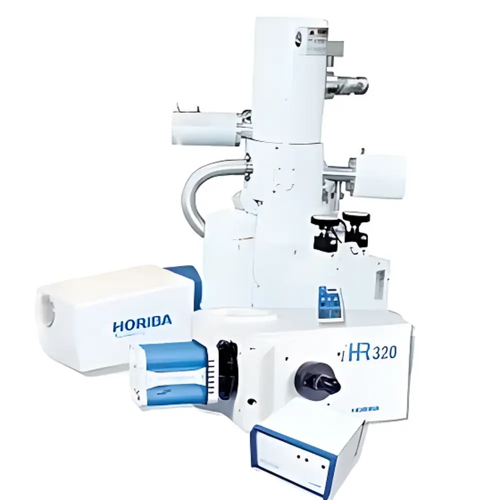
HORIBA JY Flex-CLUE Cathodoluminescence Spectroscopy System
| Brand | HORIBA |
|---|---|
| Origin | France |
| Model | Flex-CLUE |
| Spectral Range | 200–1000 nm or 400–1700 nm |
| Optical Coupling | Fiber-coupled |
| Spectrometer Focal Length Options | 140 mm, 200 mm, 320 mm |
| Grating Options | Multiple selectable |
| Measurement Modes | Point acquisition, line scan, hyperspectral mapping |
| Detector Compatibility | Open-electrode CCD, EMCCD, InGaAs arrays |
| Integration | SEM-compatible (FE-SEM, SEM, STEM) |
| Spatial Resolution | Sub-100 nm (dependent on electron beam conditions and sample properties) |
Overview
The HORIBA JY Flex-CLUE is a high-performance, fiber-coupled cathodoluminescence (CL) spectroscopy system engineered for integration with scanning electron microscopes (SEMs), field-emission SEMs (FE-SEMs), and scanning transmission electron microscopes (STEMs). It enables quantitative, spatially resolved optical emission analysis induced by electron beam excitation — a technique grounded in the physical principle that incident high-energy electrons generate electron-hole pairs in luminescent materials, whose subsequent radiative recombination emits photons characteristic of local electronic structure, defect states, impurity incorporation, and crystallographic environment. Unlike conventional photoluminescence or electroluminescence methods, CL provides nanoscale optical contrast directly correlated with structural and compositional features observed in the same instrument, making it indispensable for correlative microstructural–optical characterization. The Flex-CLUE is not a standalone spectrometer but a modular, vacuum-compatible detection platform designed for minimal footprint and maximal flexibility in constrained chamber geometries.
Key Features
- Fiber-optic coupling architecture ensures mechanical decoupling from the SEM column, eliminating vibration-induced spectral drift and enabling stable long-duration acquisitions.
- Optimized light collection efficiency across the full UV–NIR range (200–1000 nm or 400–1700 nm), achieved through high-throughput optics and anti-reflection coated fused silica or CaF2 fiber bundles.
- Modular spectrometer integration supports focal lengths of 140 mm, 200 mm, and 320 mm — balancing resolution (≤0.1 nm at 500 nm with 1200 g/mm grating), throughput, and compactness.
- Multi-grating turret allows rapid switching between dispersion configurations for optimized signal-to-noise ratio in specific spectral windows — e.g., deep-UV for wide-bandgap semiconductors or NIR for rare-earth-doped phosphors.
- Real-time synchronization with SEM scan generators enables pixel-synchronized CL mapping, including point spectra, line profiles, and full hyperspectral data cubes (λ-x-y).
- SWIFT™ ultrafast imaging mode (optional) delivers sub-millisecond dwell times per pixel without compromising spectral fidelity — critical for beam-sensitive materials such as organometallic perovskites or biological mineral phases.
Sample Compatibility & Compliance
The Flex-CLUE accommodates conductive, semi-conductive, and insulating samples — including bulk crystals, thin films, nanostructures (quantum dots, nanowires), geological specimens (zircon, calcite, dolomite), and functional ceramics. Charge compensation strategies (e.g., low-kV operation, beam deceleration, or low-vacuum mode) are fully compatible. The system adheres to IEC 61000-6-3 (EMC emissions) and IEC 61000-6-2 (immunity) standards. Data acquisition workflows support audit-trail-enabled operation under GLP and GMP frameworks when paired with HORIBA’s LabSpec 6 software configured for 21 CFR Part 11 compliance (electronic signatures, user access control, immutable metadata logging).
Software & Data Management
Controlled via HORIBA’s LabSpec 6 platform, the Flex-CLUE offers unified instrument orchestration: simultaneous SEM navigation, beam parameter definition, spectral acquisition, and real-time hyperspectral visualization. Raw data are stored in vendor-neutral HDF5 format with embedded calibration metadata (wavelength, slit width, grating ID, detector gain). Advanced processing includes spectral unmixing (via non-negative matrix factorization), peak deconvolution (Voigt fitting), spatial correlation overlays with SE/BSE images, and export to Python/MATLAB via documented APIs. Batch processing pipelines support automated quality checks for intensity stability, background subtraction consistency, and spectral centroid tracking across large-area maps.
Applications
- Semiconductor R&D: Mapping dislocation-related luminescence in GaN HEMTs, identifying SiC polytype boundaries, quantifying dopant activation in AlGaN quantum wells.
- Geosciences: Distinguishing growth zoning in zircon using U–Th–Pb age-correlated CL intensity variations; differentiating dolomite from calcite based on Mn2+/Fe2+ luminescence ratios.
- Advanced Ceramics: Correlating grain boundary segregation (e.g., Yb3+ in YAG) with localized emission quenching; assessing sintering homogeneity in transparent alumina via CL intensity uniformity.
- Photonics & Nanophotonics: Characterizing Purcell enhancement in plasmonic nanoantennas; validating band-edge emission shifts in colloidal perovskite nanocrystals.
- Forensic Materials Analysis: Discriminating synthetic vs. natural gemstones (e.g., diamond HPHT treatment signatures); identifying trace-element fingerprints in glass fragments.
FAQ
Is the Flex-CLUE compatible with my existing SEM model?
Yes — the system interfaces via standard TTL/RS-232 or Ethernet protocols with major SEM platforms (Thermo Fisher, Zeiss, JEOL, Hitachi) and supports custom trigger logic for legacy instruments.
Can I perform time-resolved CL measurements with this system?
Time-resolved capability requires optional pulsed electron gun synchronization and fast-gated detectors (e.g., MCP-CCD or SPAD arrays); the Flex-CLUE’s fiber interface and timing electronics are pre-engineered for such upgrades.
What vacuum requirements apply to the optical path?
The fiber feedthrough maintains UHV compatibility (<1×10⁻⁷ mbar) and uses metal-sealed CF flanges; no additional pumping is needed beyond the host SEM chamber.
How is spectral calibration maintained during long-term operation?
LabSpec 6 performs automatic wavelength calibration using built-in Hg/Ar lamp references before each session, with optional in-situ recalibration using known sample emission lines (e.g., Si Raman at 520.7 cm−1).
Does HORIBA provide application-specific method templates?
Yes — validated SOPs are available for semiconductor defect mapping, geological phase identification, and ceramic grain boundary analysis, including instrument setup files, processing scripts, and reporting templates compliant with ISO/IEC 17025 documentation requirements.