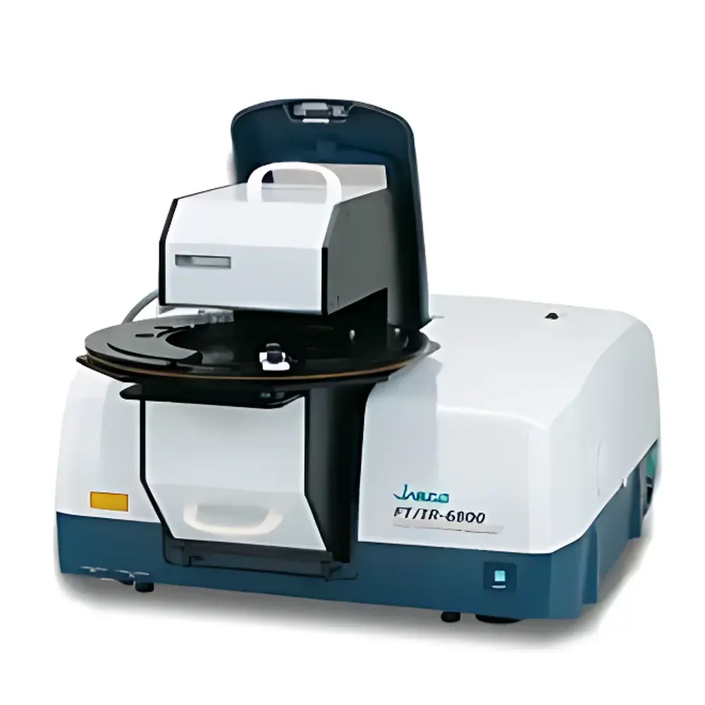
JASCO FT/IR-4000 & FT/IR-6000 Series Wafer Reflectance Measurement System
| Brand | JASCO |
|---|---|
| Origin | Japan |
| Model | FT/IR-4000, FT/IR-6000 Series |
| Instrument Type | Laboratory Fourier Transform Infrared (FTIR) Spectrometer |
| Wavenumber Range | 7800–400 cm⁻¹ |
| Spectral Resolution | 0.4 cm⁻¹ |
| Signal-to-Noise Ratio (S/N) | 55,000:1 (at 4 cm⁻¹, 1 min scan, MCT detector) |
| Sample Compatibility | Up to 300 mm (12″) silicon wafers |
| Measurement Modes | Specular reflectance, transmission, and attenuated total reflectance (ATR) with wafer-specific accessories |
| Compliance | JEITA RC-2001, JEIDA-6301, SEMI F39, ASTM F1597, ISO 14644-1 (cleanroom-compatible operation) |
Overview
The JASCO FT/IR-4000 and FT/IR-6000 Series Wafer Reflectance Measurement Systems are high-performance, laboratory-grade Fourier Transform Infrared (FTIR) spectrometers engineered specifically for quantitative metrology of semiconductor silicon wafers. These systems operate on the principle of interferometric spectral acquisition—measuring infrared absorption and reflection signatures across a broad wavenumber range (7800–400 cm⁻¹) to detect and quantify trace interstitial oxygen (Oi), substitutional carbon (Cs), nitrogen (N), and hydrogen-related species (e.g., Si–H, Si–H2) in crystalline silicon substrates. The optical architecture integrates a thermally stabilized Michelson interferometer, high-efficiency KBr or CaF2 beam splitter, and liquid-nitrogen-cooled mercury cadmium telluride (MCT) detector, delivering exceptional signal fidelity and long-term baseline stability required for process-critical wafer characterization.
Key Features
- Optimized optical path design for specular reflectance measurements on flat, polished silicon wafers up to 300 mm (12″) diameter—minimizing stray light and angular sensitivity artifacts.
- Automated wafer stage with precision XYZ translation and theta rotation, enabling repeatable positioning for multi-point mapping and edge profiling.
- High-resolution spectral acquisition at ≤0.4 cm⁻¹ unapodized resolution, supporting accurate peak deconvolution of overlapping vibrational bands (e.g., Oi at 1107 cm⁻¹ and Cs at 605 cm⁻¹).
- Signal-to-noise ratio exceeding 55,000:1 (4 cm⁻¹, 1-minute scan, MCT detector), ensuring robust detection limits for low-concentration dopants and contaminants.
- Dual-beam referencing capability with integrated background collection from bare silicon reference wafers, correcting for instrumental drift and substrate thickness interference effects.
- Modular accessory interface compliant with JASCO’s universal optical bench, allowing seamless integration of polarization optics, variable-angle reflectance stages, and cryogenic sample holders.
Sample Compatibility & Compliance
The system accommodates standard semiconductor wafer formats (100 mm to 300 mm), including prime, test, and monitor wafers with native oxide, thermal oxide, or deposited dielectric layers (SiO2, SiNx). It supports both front-side and back-side reflectance configurations without physical contact—preserving surface integrity and eliminating risk of particle generation. All measurement protocols and calibration routines conform to industry-standard specifications: JEITA RC-2001 (Oi quantification), JEIDA-6301 (carbon analysis), SEMI F39 (infrared spectroscopy for silicon), and ASTM F1597 (standard test method for interstitial oxygen in silicon by FTIR). The instrument platform is designed for Class 100 cleanroom environments (ISO 14644-1) and supports GLP/GMP-aligned audit trails when operated with validated software configurations.
Software & Data Management
JASCO’s Spectra Manager™ II software provides a dedicated Wafer Analysis Module with preconfigured methods for oxygen, carbon, and hydrogen quantification per JEITA/SEMI guidelines. The module includes automated baseline correction using polynomial or rubberband algorithms, peak fitting with constrained Gaussian–Lorentzian models, and stoichiometric conversion using published absorption coefficients (e.g., 3.14 × 10¹⁷ cm⁻²·ppma⁻¹ for Oi). All raw interferograms, spectra, and processed results are stored in vendor-neutral HDF5 format with embedded metadata (date/time, operator ID, instrument serial number, calibration status). Audit trail functionality complies with FDA 21 CFR Part 11 requirements when deployed with electronic signature and role-based access control enabled.
Applications
- Quantitative determination of interstitial oxygen concentration in Czochralski-grown silicon wafers for crystal growth process control.
- Measurement of substitutional carbon content to assess ingot homogeneity and thermal budget impact during device fabrication.
- Hydrogen passivation analysis in plasma-enhanced chemical vapor deposition (PECVD) SiNx capping layers.
- Monitoring of native oxide thickness and quality via Si–O stretching mode intensity ratios (1070 cm⁻¹ / 800 cm⁻¹).
- Failure analysis of gate oxide integrity through detection of moisture-induced hydroxyl (OH) peaks near 3500 cm⁻¹.
- Supporting process qualification for advanced nodes (≤28 nm) where trace impurity levels directly influence leakage current and threshold voltage stability.
FAQ
What wafer sizes does the system support?
The system accommodates wafers from 100 mm (4″) up to 300 mm (12″) in diameter using motorized, vacuum-chuck stages with positional repeatability better than ±2 µm.
Is calibration traceable to NIST standards?
Yes—wavenumber calibration is performed using polystyrene film reference standards certified to NIST SRM 1921b; absorbance linearity verified per ASTM E1421.
Can the system perform mapping across the wafer surface?
Yes—integrated XY scanning stage enables automated grid-based reflectance acquisition at user-defined step intervals (minimum 1 mm), with real-time spectral preview and outlier rejection.
Does the software support automated pass/fail reporting per JEITA RC-2001?
Yes—the Wafer Analysis Module generates compliance reports with embedded uncertainty estimates, measurement uncertainty budgets, and deviation flags aligned to JEITA tolerance thresholds.
What detector options are available for enhanced sensitivity in the mid-IR region?
Standard configuration uses liquid-N2-cooled MCT; optional dual-detector modules (MCT + DTGS) enable rapid switching between high-sensitivity and wide-dynamic-range modes without realignment.

")
")