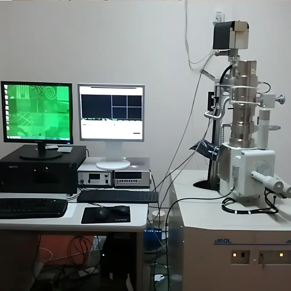
JC Nabity NPGS V9.2 Nanometer Pattern Generation System (EBL Add-on for SEM/STEM/FIB)
| Brand | JC Nabity |
|---|---|
| Origin | USA |
| Model | NPGS V9.2 |
| Minimum Feature Size | 10 nm |
| Electron Beam Diameter | ≤1 nm |
| Accelerating Voltage Range | 0–40 kV |
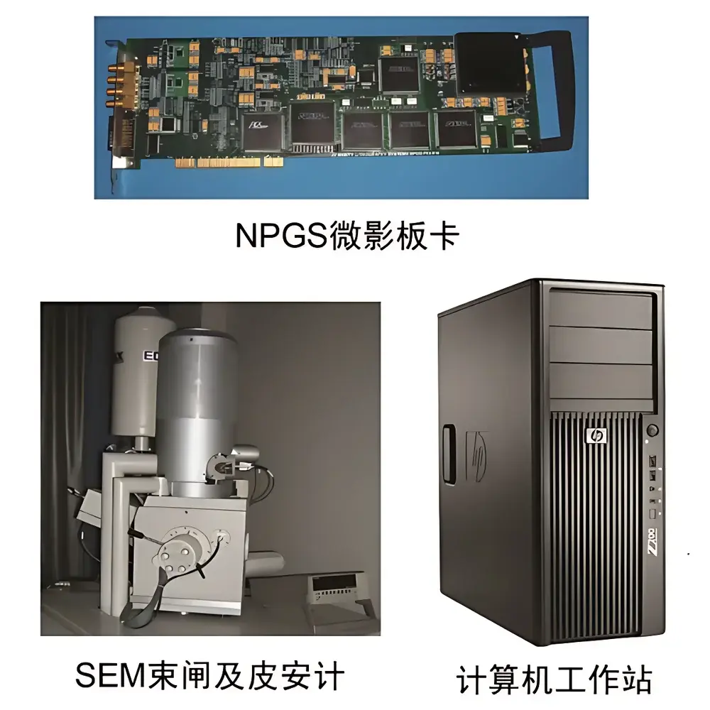
| Control Interface | PCIe-516A High-Speed Lithography Board |
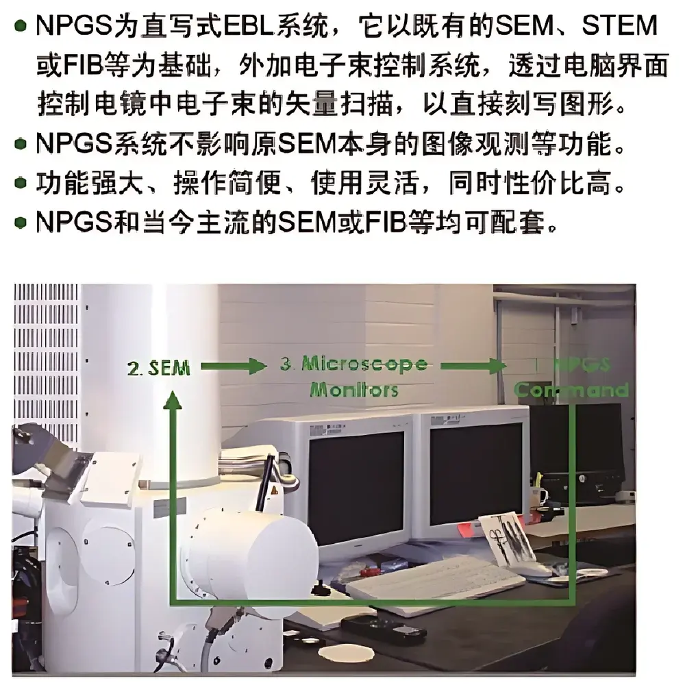
| Host Compatibility | Commercial SEM, STEM, or FIB Systems |
| Operating System | Windows 10 |
| Pattern Design Software | QCAD |
| Beam Blanking Frequency | Up to 5 MHz |
Overview
The JC Nabity NPGS V9.2 Nanometer Pattern Generation System is a high-precision electron beam lithography (EBL) add-on platform engineered to convert commercially available scanning electron microscopes (SEM), scanning transmission electron microscopes (STEM), or focused ion beam (FIB) systems into fully functional direct-write nanofabrication tools. Unlike standalone EBL tools requiring dedicated vacuum chambers and electron optics, the NPGS leverages the existing electron column, detectors, and stage of host instruments—retaining full imaging capability while enabling sub-10 nm pattern definition via vector-scan beam control. Its operational principle relies on Coulomb-limited electron beam focusing and electrostatic/magnetic blanking at up to 5 MHz, exploiting the short de Broglie wavelength (<0.01 nm at 30 kV) to circumvent optical diffraction limits. Designed explicitly for research-grade nanofabrication, the system supports both positive (e.g., PMMA) and chemically amplified negative resists, with dose calibration traceable to primary standards via integrated picoammeter feedback (Keithley 6485). It is not intended for high-throughput production but delivers reproducible, metrology-ready patterning for maskless prototyping in academic, national lab, and R&D environments.
Key Features
- Modular PCIe-based lithography controller (NPGS PCIe-516A) with 16-bit DAC resolution and 0.25% linearity, synchronized to host microscope scan coils
- Real-time beam blanking with ≤20 ns rise/fall time and stable duty-cycle control across 1 Hz–5 MHz frequency range
- Automated field stitching and overlay alignment using stage encoder feedback and fiducial-based registration
- Integrated beam current monitoring via calibrated picoammeter (Keithley 6485), enabling closed-loop dose control per exposure field
- Vector-scan mode prioritizes pattern geometry over raster grid, reducing write time by >70% for sparse layouts versus conventional raster scanning
- Compatible with standard SEM/FIB stages (including piezo-driven and laser-interferometric models), supporting Z-height compensation during multi-field exposure
- Native support for common CAD formats (DXF, GDSII, CIF) and parametric shape generation within QCAD pattern editor
Sample Compatibility & Compliance
The NPGS V9.2 operates exclusively on conductive or charge-dissipative substrates mounted on standard SEM stubs or TEM grids. Compatible resist systems include polymethyl methacrylate (PMMA), hydrogen silsesquioxane (HSQ), ZEP-520A, and chemically amplified resists such as ma-N 2400 series. Substrate materials span silicon wafers, SOI, GaAs, sapphire, quartz, and 2D materials (graphene, MoS₂) transferred onto TEM grids. The system complies with general laboratory electromagnetic compatibility (EMC) standards (IEC 61326-1) and meets electrical safety requirements per UL 61010-1. While not certified for ISO 13485 or FDA 21 CFR Part 11 out-of-the-box, audit-ready software logging—including timestamped exposure logs, beam current traces, and stage position histories—is enabled through optional configuration for GLP/GMP-aligned workflows. All resist processing steps (spin-coating, baking, development, etch transfer) remain external to the NPGS and must follow established cleanroom protocols aligned with ISO 14644-1 Class 5 or better.
Software & Data Management
NPGS V9.2 runs on Windows 10 x64 with deterministic real-time kernel extensions for low-latency beam control. The core lithography engine provides hierarchical pattern compilation, proximity effect correction (PEC) via variable-shaped beam dose modulation, and dynamic focus compensation based on topographic height maps imported from SEM secondary electron images. QCAD serves as the native layout editor, supporting Boolean operations, array generation, and script-driven automation (Python API). Exposure job files (.npf) embed full metadata: beam energy, working distance, magnification, dwell time, and resist sensitivity parameters. All system events—including blanker state transitions, stage moves, and current measurements—are logged to SQLite databases with SHA-256 checksums for integrity verification. Export options include industry-standard GDSII stream files with layer mapping, enabling seamless handoff to mask shops or downstream process simulation tools (e.g., Sentaurus Lithography, Silvaco ACT).
Applications
The NPGS V9.2 serves as a foundational tool for nanoscale device prototyping across multiple domains. In semiconductor research, it enables rapid iteration of test structures for novel transistor architectures (nanowires, FinFETs, gate-all-around devices), plasmonic metasurfaces, and quantum dot arrays. For MEMS/NEMS development, it facilitates fabrication of high-aspect-ratio comb drives, nanomechanical resonators, and fluidic channel masters with critical dimensions down to 10 nm. In quantum technologies, researchers use it to define superconducting nanowire single-photon detectors (SNSPDs), flux qubit test chips, and spin-qubit gate electrodes on isotopically purified silicon. Its integration with plasma etch (ICP-RIE), PECVD, and sputtering tools allows full process flow execution—from pattern definition to functional device release—within shared cleanroom infrastructure. Notably, its ability to perform in situ SEM imaging before and after exposure enables iterative process optimization without sample removal.
FAQ
Can NPGS V9.2 be used with any SEM model?
Yes—provided the SEM offers analog scan coil inputs (X/Y deflection voltages) and a TTL-compatible blanking port. Compatibility has been verified with JEOL, Thermo Fisher Scientific (FEI), Zeiss, Hitachi, and Tescan platforms. Custom interface adapters are available for legacy or proprietary systems.
Does NPGS support automatic focus or astigmatism correction during writing?
No—focus and stigmation must be manually optimized prior to exposure. However, the system supports Z-stage height mapping and stores focus offsets per field to compensate for substrate tilt or curvature.
Is proximity effect correction (PEC) included?
Yes—NPGS V9.2 includes built-in PEC algorithms based on point-spread function convolution and dose matrix inversion. Users may import empirical scattering kernels or apply default models for PMMA on Si/SiO₂.
What is the typical throughput for a 10 µm × 10 µm field at 10 nm resolution?
At 30 kV, 100 pA beam current, and 10 µC/cm² dose in PMMA, write time ranges from 2.5 to 6 minutes depending on pattern density and blanking efficiency—consistent with peer-reviewed benchmarks for similar add-on EBL systems.
Are software updates and technical support included post-purchase?
JC Nabity provides 12 months of complimentary software maintenance and remote engineering support. Extended support contracts and on-site installation/calibration services are available upon request.


