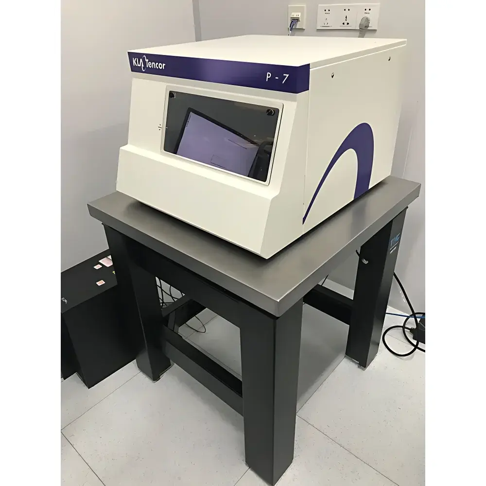
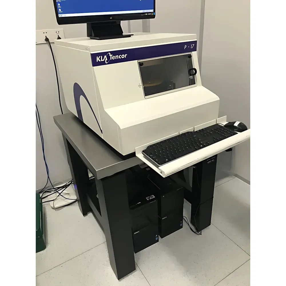
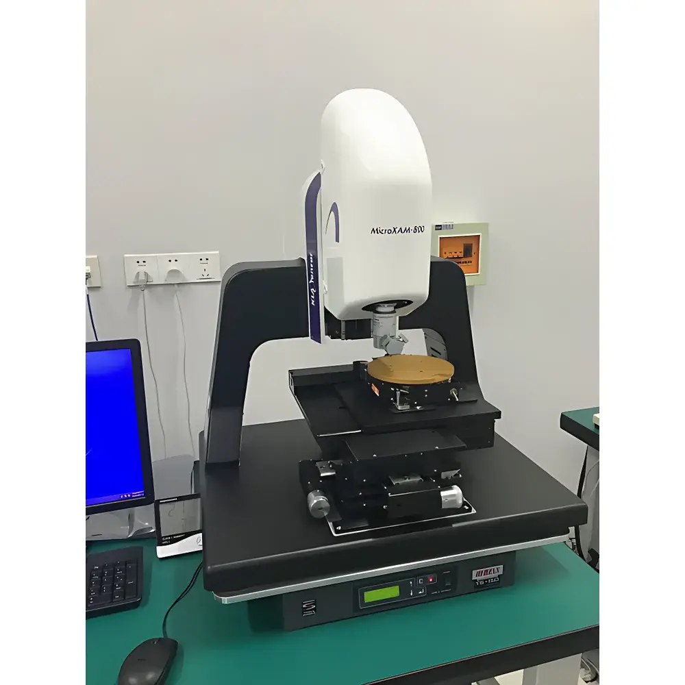
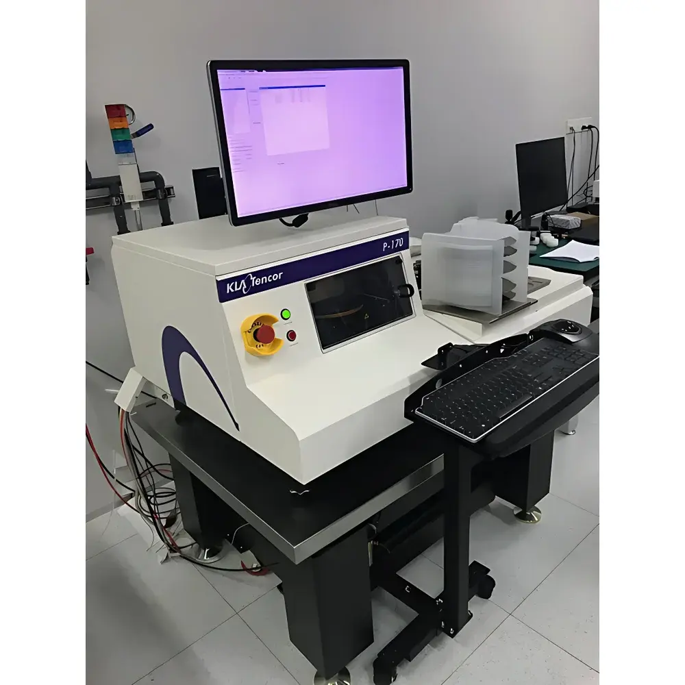
KLA D-500/600 and P-7/P-17 Contact Profilometers
| Brand | KLA |
|---|---|
| Origin | Malaysia |
| Product Type | Contact Profilometer / Surface Roughness Tester |
| Operating Principle | Stylus-Based Profilometry |
| Model Range | D-500, D-600, P-7, P-17 |
| Compliance | Designed for ISO 25178, ISO 4287, ASTM E1093, USP <1056>, and GLP/GMP-aligned workflows |
Overview
The KLA D-500, D-600, P-7, and P-17 are high-precision contact profilometers engineered for quantitative surface topography characterization in research and industrial quality control environments. These instruments operate on the established principle of stylus-based profilometry—where a diamond-tipped probe traverses the sample surface under controlled force, converting vertical displacement into analog voltage signals via a linear variable differential transformer (LVDT) or piezoresistive sensor. The resulting profile data enables traceable, NIST-referenced measurement of step height, surface roughness (Ra, Rq, Rz), waviness, curvature, slope, and thin-film stress-induced deformation. Developed by KLA—a global leader in semiconductor process control and metrology—the D- and P-series systems integrate decades of expertise in micro/nanoscale surface metrology, with hardware architecture optimized for long-term dimensional stability, thermal drift compensation, and mechanical repeatability across multi-shift manufacturing and regulated laboratory settings.
Key Features
- Modular platform architecture supporting interchangeable scanning stages (linear, rotary, and XYZ motorized), enabling both localized line scans and full-field grid mapping up to 200 mm × 200 mm
- Diamond stylus options with tip radii ranging from 2 µm to 12.5 µm, selectable based on surface hardness and feature resolution requirements
- Vertical resolution down to 0.1 nm (D-600) and lateral resolution ≤ 100 nm, calibrated per ISO 25178-601 using certified step-height standards
- Programmable scan speed (0.1–5 mm/s) and normal force (0.5–5 mN), adjustable in real time to accommodate soft polymers, brittle oxides, or ductile metals
- Vibration-isolated granite base with active air suspension, reducing environmental noise coupling during sub-nanometer vertical measurements
- Integrated environmental monitoring (temperature, humidity) linked to software-based drift correction algorithms
Sample Compatibility & Compliance
These profilometers accept rigid and semi-rigid substrates including silicon wafers, sapphire, fused silica, stainless steel, aluminum alloys, photoresists, spin-coated polymer films, and MEMS devices. Sample thickness ranges from 0.1 mm to 50 mm; maximum weight capacity is 5 kg. All D- and P-series systems are configured to support compliance with international metrology standards: ISO 25178-2 (areal surface texture parameters), ISO 4287 (profile-based roughness), ASTM E1093 (step height verification), and USP for pharmaceutical surface characterization. Audit-ready data logging—including operator ID, instrument calibration status, environmental conditions, and timestamped raw profile traces—meets FDA 21 CFR Part 11 requirements when deployed with KLA’s validated software suite.
Software & Data Management
Operation is managed through KLA’s proprietary NanoView™ software platform, which provides intuitive workflow-driven interfaces for measurement setup, real-time feedback, automated report generation, and statistical process control (SPC) charting. Raw profile data is stored in vendor-neutral .csv and .xml formats, with metadata embedded per ASTM E1394. Advanced analysis modules include power spectral density (PSD) computation, bearing ratio curve (Abbott-Firestone), grain boundary detection, and film stress modeling using Stoney’s equation. Software validation documentation, IQ/OQ protocols, and electronic signature functionality are available upon request for GxP-regulated users.
Applications
The D-500/600 and P-7/17 systems serve as primary metrology tools across multiple domains: semiconductor process development (etch depth, CMP uniformity, lithographic resist profiles); advanced packaging (copper pillar height, under-bump metallization roughness); thin-film solar cell characterization (TCO layer morphology, interface step coverage); biomedical device surface engineering (stent strut roughness, hydrogel swelling topography); and academic nanomaterials research (2D material flake thickness, graphene transfer defects). Their ability to correlate nanoscale topography with functional performance—such as electrical contact resistance or adhesion strength—makes them indispensable in cross-disciplinary labs pursuing structure-property relationships.
FAQ
What stylus tip radius is recommended for measuring soft polymer films?
A 2 µm radius diamond stylus operating at ≤1 mN normal force is typically used for compliant organic layers to minimize plastic deformation.
Can these systems measure transparent or reflective surfaces without optical interference?
Yes—contact profilometry is inherently insensitive to optical properties, making it ideal for measuring anti-reflective coatings, ITO layers, and deep-UV lithography masks.
Is traceable calibration support available for ISO/IEC 17025-accredited labs?
KLA provides factory-certified calibration kits (NIST-traceable step standards), along with on-site calibration services performed by ISO/IEC 17025-accredited engineers.
How does the system handle thermal drift during extended overnight measurements?
Real-time temperature compensation algorithms adjust vertical gain and zero offset continuously, while the granite base’s low coefficient of thermal expansion (<2 µm/m·°C) minimizes mechanical drift.
Are there options for integrating profilometry data into existing MES or LIMS platforms?
Yes—NanoView™ supports OPC UA and RESTful API interfaces for bidirectional data exchange with enterprise manufacturing execution and laboratory information management systems.