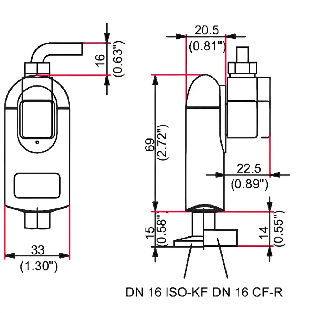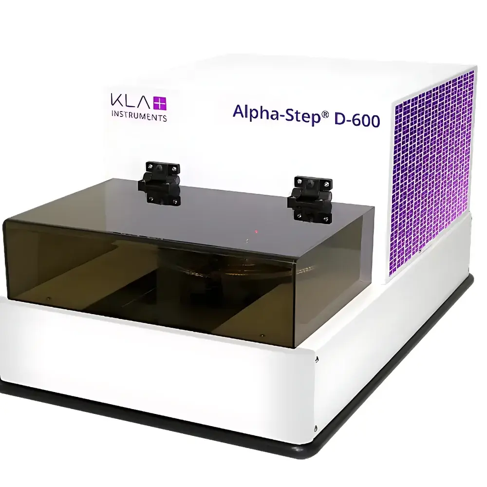
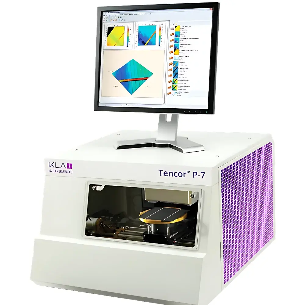
KLA Alpha-Step D600/P-7 Advanced Stylus Profilometer
| Brand | KLA |
|---|---|
| Origin | Malaysia |
| Model | D600/P-7 |
| Measurement Principle | Mechanical Stylus Profiling with Optical Reflectance Height Detection |
| Vertical Measurement Range | 0.1 nm to 1200 µm |
| Vertical Accuracy | ±0.1 µm |
| Probe Normal Force | 0.03–15 mg |
| Maximum Scan Length | 55 mm (D600), 150 mm (P-7) |
| Step Height Repeatability | 0.10% (1σ) |
| Vertical Resolution | 0.38 Å |
| Maximum Sample Size | 200 mm diameter |
Overview
The KLA Alpha-Step D600 and P-7 are high-precision mechanical stylus profilometers engineered for traceable, quantitative surface topography characterization in semiconductor process development, thin-film metrology, MEMS fabrication, and advanced materials R&D. Operating on the principle of physical stylus contact combined with optical reflectance-based vertical displacement sensing, these instruments deliver sub-angstrom vertical resolution and nanometer-level step height accuracy without reliance on optical interference or diffraction effects. Unlike non-contact optical profilers, the Alpha-Step platform maintains measurement fidelity across low-reflectivity, transparent, or highly textured surfaces—critical for characterizing photoresist profiles, etch depth uniformity, metal film stress-induced curvature, and atomic-layer-deposited (ALD) step coverage. The system’s electromagnetic force feedback control ensures consistent, programmable probe loading—enabling repeatable profiling of soft polymer films, organic semiconductors, and low-modulus dielectrics without plastic deformation or tip wear artifacts.
Key Features
- Sub-angstrom vertical resolution (0.38 Å RMS) achieved via ultra-stable UltraLite® sensor architecture with integrated thermal drift compensation and closed-loop Z-axis positioning.
- Programmable probe normal force from 0.03 mg to 15 mg—optimized for fragile layers (e.g., spin-on carbon, SU-8, PEDOT:PSS) while maintaining signal-to-noise integrity on hard substrates (Si, SiO₂, sapphire).
- Dual-platform flexibility: D600 features a motorized X-Y stage with 55 mm maximum scan length and integrated optical height detection; P-7 extends capability with a 150 mm × 150 mm closed-loop automated stage and extended scan range—enabling full-wafer edge-to-edge profiling with stitching capability.
- 0.10% (1σ) step height repeatability—validated per ISO 25178-601 and ASTM E2942 protocols—ensuring statistical confidence in process control limits and SPC implementation.
- Robust mechanical design with granite base, air-isolated vibration damping, and environmental enclosure options for cleanroom-compatible operation (Class 100/ISO 5 compliant installations).
Sample Compatibility & Compliance
The Alpha-Step D600/P-7 accommodates wafers up to 200 mm in diameter and standard SEM stubs, TEM grids, glass slides, and flexible substrates (e.g., PET, PI). Surface types include bare silicon, patterned oxides, metal stacks (Al, Cu, TiN), low-k dielectrics, photoresists (positive/negative tone), OLED encapsulation layers, and biomedical coatings. All measurements adhere to ISO 25178-2 (areal surface texture parameters), ISO 4287 (profile parameters), and ASTM E1399 (step height calibration standards). Data acquisition and reporting support GLP/GMP audit trails, including electronic signatures, user access controls, and 21 CFR Part 11-compliant software validation packages upon request.
Software & Data Management
Acquired data is processed using KLA’s proprietary Vision64™ software, which provides ISO-compliant parameter calculation (Sa, Sq, Sz, Sp, Sv, Sdr, etc.), multi-layer film thickness deconvolution, stress-induced curvature modeling (Stoney equation integration), and cross-sectional roughness/waviness separation via digital filtering (Gaussian, spline, robust polynomial). Raw profile data exports in ASCII, CSV, and Metrology Data Exchange Format (MDEF) for integration into factory MES systems (e.g., Applied Materials Endura, Lam Research Flex). Software supports batch recipe automation, pass/fail thresholding with color-coded overlay maps, and PDF report generation with embedded metadata (operator ID, timestamp, calibration certificate ID, environmental log).
Applications
- Semiconductor: Etch depth uniformity on 300 mm wafers, resist develop rate monitoring, CMP endpoint verification, TSV sidewall step coverage quantification.
- Display & Flexible Electronics: ITO film thickness on curved substrates, OLED pixel bank height consistency, touch sensor electrode step height tolerance validation.
- MEMS & Sensors: Cantilever deflection profiling under thermal load, piezoelectric film stress mapping, microfluidic channel depth verification.
- Advanced Packaging: Under-bump metallization (UBM) step height post-reflow, redistribution layer (RDL) planarity assessment, fan-out wafer-level packaging (FOWLP) warpage correlation.
- Materials Science: Thin-film adhesion failure analysis via scratch profiling, corrosion pit depth distribution, battery electrode coating thickness gradients.
FAQ
What is the difference between the D600 and P-7 models?
The D600 is optimized for high-resolution, short-range scanning (≤55 mm) with enhanced optical height detection for rapid alignment and shallow feature profiling. The P-7 prioritizes large-area metrology with its 150 mm × 150 mm closed-loop stage, enabling full-die or multi-die stitching and long-range waviness analysis.
Can the system measure transparent or semi-transparent films?
Yes—unlike optical interferometers, the mechanical stylus method is insensitive to optical properties. Film thickness and interface steps are resolved directly via physical contact, making it suitable for SiO₂ on Si, polymer-on-glass, or DLC-on-metal stacks.
Is calibration traceable to NIST or other national standards?
All factory calibrations are performed using NIST-traceable step height standards (e.g., NIST SRM 2160, 2161) and documented in accordance with ISO/IEC 17025 requirements. On-site recalibration services include uncertainty budgets per GUM (JCGM 100:2008).
Does the software support automated SPC charting?
Yes—Vision64 includes real-time X-bar/R charting, Cpk/Ppk calculation, and assignable cause flagging based on user-defined control limits, fully compliant with IATF 16949 and JEDEC JESD22-A108 reliability test reporting structures.