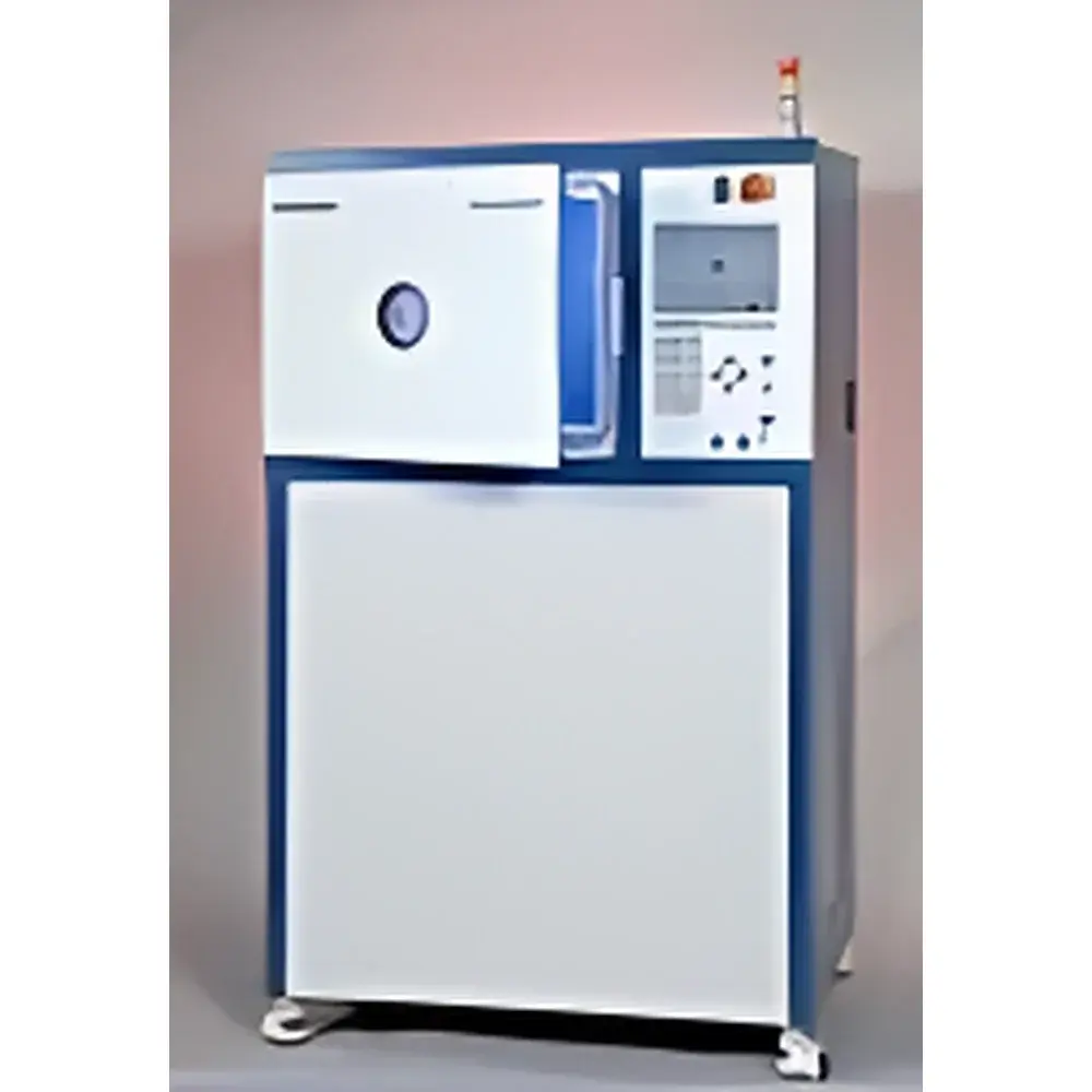
PVA TePla GIGA 690 Microwave Plasma Cleaning System
| Brand | PVA TePla |
|---|---|
| Origin | Germany |
| Model | GIGA 690 |
| Instrument Type | Imported Microwave Plasma Cleaner |
| Category | Plasma Surface Treater for Sample Preparation |
Overview
The PVA TePla GIGA 690 is a high-precision microwave-driven plasma cleaning system engineered for ultra-clean surface activation, organic residue removal, and oxide reduction in demanding R&D and production environments. Operating at 2.45 GHz microwave frequency, the system generates stable, high-density non-thermal plasma without internal electrodes—eliminating contamination risks associated with capacitive or RF plasma sources. Unlike low-power benchtop plasma units, the GIGA 690 delivers uniform plasma distribution across large-area substrates (up to 690 mm diameter), making it suitable for wafer-level processing, ceramic substrate conditioning, and advanced packaging preparation. Its vacuum-integrated architecture ensures reproducible process control under pressures ranging from 10⁻² to 10 mbar, compatible with argon, oxygen, hydrogen, nitrogen, and forming gas chemistries. Designed and manufactured in Germany, the system complies with CE directives and integrates seamlessly into cleanroom-class Class 100–Class 1000 environments.
Key Features
- Microwave plasma generation (2.45 GHz) with magnetron power regulation (0–3 kW continuous, adjustable in 10 W increments)
- Large-diameter process chamber (Ø690 mm × H450 mm) with quartz-lined cylindrical cavity for uniform field distribution
- Integrated turbomolecular pumping station (base pressure ≤5×10⁻⁷ mbar) coupled with precise mass flow controllers (MFCs) for multi-gas delivery (O₂, Ar, H₂, N₂, CF₄, forming gas)
- Programmable process sequencing via industrial PLC with up to 99 user-defined recipes, each supporting multi-step pressure/power/gas ramping
- Real-time monitoring of reflected power, forward power, chamber pressure, and gas temperature via calibrated sensors with 0.1% full-scale accuracy
- Interlocked safety architecture compliant with EN 61000-6-2 (EMC immunity) and EN 61000-6-4 (EMC emission) standards
Sample Compatibility & Compliance
The GIGA 690 accommodates rigid and flexible substrates including silicon wafers (up to 300 mm), glass carriers (e.g., FPD, OLED backplanes), ceramic packages (LTCC/HTCC), metal leadframes, polymer films (PI, PET, PC), and composite laminates. Surface treatment is fully compatible with subsequent thin-film deposition (PVD, CVD), wire bonding, die attach, and conformal coating processes. The system supports traceable process validation per ISO 14644-1 (cleanroom classification), ASTM F209 (cleanliness testing), and SEMI S2/S8 safety guidelines. For regulated industries, optional audit trail logging and electronic signature modules align with FDA 21 CFR Part 11 requirements when integrated with validated LIMS or MES platforms.
Software & Data Management
Control is executed through PVA TePla’s proprietary PlasmaControl™ v5.2 software, running on an embedded industrial PC with Windows IoT Enterprise OS. The interface provides real-time graphical display of plasma parameters, historical trend logging (≥1 year at 1 Hz resolution), and CSV/Excel export with time-stamped metadata (operator ID, recipe version, chamber history). All process data are stored locally with RAID-1 redundancy and support optional network backup to secure NAS or cloud-based storage. Remote diagnostics via TLS-encrypted VNC connection enable technical support without compromising firewall integrity. Software updates follow IEC 62304-compliant development lifecycle and include full revision history and change logs traceable to individual firmware builds.
Applications
- Semiconductor: Removal of photoresist residuals, post-etch polymer scum, and native oxide prior to ALD or epitaxy
- MEMS & Sensors: Hydrophilization of SiO₂ and SiN surfaces to improve adhesive bond strength and reduce delamination
- Medical Devices: Sterilization-grade surface activation of polymeric catheters, microfluidic chips, and implantable housings
- Optics & Photonics: Cleaning of fused silica and sapphire substrates prior to anti-reflective coating deposition
- Advanced Packaging: Activation of mold compound surfaces and underfill interfaces to enhance interfacial adhesion and moisture resistance
- Research: In-situ surface functionalization (e.g., amine grafting via NH₃ plasma) for biosensor development and nanomaterial integration
FAQ
What vacuum level is required for stable microwave plasma ignition?
Stable plasma ignition is achieved between 1×10⁻² and 5×10⁻¹ mbar; optimal cleaning uniformity occurs at 1–3×10⁻¹ mbar for O₂-based processes.
Can the GIGA 690 handle 300 mm wafers with edge exclusion control?
Yes—the system supports full-wafer processing with programmable edge exclusion zones (0.5–5 mm) via adjustable electrode shielding and localized gas injection.
Is remote operation supported for unattended overnight runs?
Yes—fully automated batch processing with email/SNMP alerts upon completion or fault detection is standard; no local operator presence required.
How is process repeatability verified across multiple chambers?
Each unit undergoes factory calibration using certified quartz crystal microbalances (QCM) and XPS reference samples; cross-chamber correlation is maintained within ±2.3% etch rate deviation (SiO₂ @ 100 W, O₂, 100 mTorr).
Does the system meet semiconductor industry ESD protection standards?
Yes—chamber grounding resistance <1 Ω, static-dissipative interior coatings, and Faraday-cage shielding ensure compliance with ANSI/ESD S20.20 and JEDEC J-STD-033.


