Sinton Instruments BCT400 Minority Carrier Lifetime Tester
| Brand | Sinton Instruments |
|---|---|
| Origin | USA |
| Model | BCT400 |
| Pricing | Upon Request |
Overview
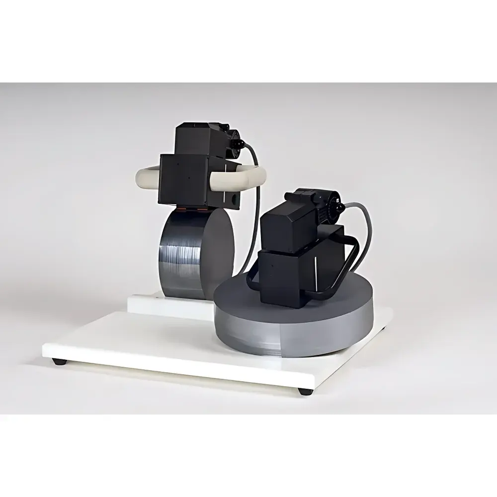
The Sinton Instruments BCT400 is a contactless, steady-state photoconductance (PC) based minority carrier lifetime tester engineered for rapid, non-destructive evaluation of bulk recombination properties in silicon wafers, ingots, and bricks. Unlike transient techniques such as microwave photoconductance decay (μ-PCD) or time-resolved photoluminescence (TRPL), the BCT400 operates on the principle of quasi-steady-state photoconductance (QSSPC), where a calibrated light source generates a stable excess carrier population, and the resulting photoconductance is measured via two-point or four-point probe configurations. This method enables direct extraction of effective minority carrier lifetime (τeff) without requiring surface passivation, oxide growth, or metal deposition—making it uniquely suited for inline process monitoring, feedstock qualification, and R&D screening of as-cut or saw-damaged silicon material.
Key Features
- Contactless, non-destructive measurement of effective minority carrier lifetime across bare silicon surfaces—no surface passivation, thermal oxidation, or metallization required.
- Optimized for large-area samples: accommodates flat, unpolished surfaces with minimum diameter of 150 mm, enabling direct assessment of as-sawn ingot cross-sections and multicrystalline bricks.
- Integrated, temperature-stabilized halogen lamp illumination with spectral output matched to silicon’s absorption profile (350–1100 nm), ensuring uniform excitation and minimal thermal drift.
- High signal-to-noise ratio electronics with auto-ranging current amplification and low-noise analog front-end, supporting lifetime measurements from sub-microsecond to >10 ms with high reproducibility.
- Rugged benchtop architecture with EMI-shielded enclosure and vibration-damped optical platform—designed for factory floor deployment and shared lab environments.
- Calibration traceable to NIST-certified reference cells and validated against ASTM F1632-21 (Standard Test Method for Measuring Minority-Carrier Lifetime of Silicon Wafers by Quasi-Steady-State Photoconductance).
Sample Compatibility & Compliance
The BCT400 accepts planar silicon specimens including monocrystalline and multicrystalline ingots, bricks, wafers, and kerf-loss samples with thickness ≥ 0.5 mm and surface flatness ≤ 50 µm peak-to-valley over 150 mm diameter. It supports both p-type and n-type Czochralski (CZ), float-zone (FZ), and cast silicon substrates with resistivity ranging from 0.1–100 Ω·cm. The system complies with ISO/IEC 17025 general requirements for calibration laboratories and supports GLP-compliant operation through audit-trail-enabled software logging. All measurement protocols align with industry-standard semiconductor metrology practices defined in SEMI MF-1530 and IEC 62788-5-1 (Photovoltaic materials — Measurement of minority-carrier lifetime in silicon wafers).
Software & Data Management
The BCT400 is operated via Sinton’s proprietary LifetimeStudio™ software, a Windows-based application supporting real-time data acquisition, spatial lifetime mapping (via optional motorized X-Y stage), and statistical batch analysis. Software features include automated dark-current compensation, intensity normalization against reference diode, and τeff calculation using the generalized QSSPC equation incorporating series resistance correction. All raw and processed datasets are stored in HDF5 format with embedded metadata (sample ID, illumination intensity, temperature, operator, timestamp). LifetimeStudio™ supports 21 CFR Part 11 compliance packages—including electronic signatures, role-based access control, and immutable audit trails—for regulated manufacturing environments subject to FDA or IATF 16949 requirements.
Applications
- Feedstock qualification: Rapid sorting of silicon ingots and bricks prior to wafering based on bulk lifetime distribution and defect density gradients.
- Crystal growth optimization: Correlation of furnace parameters (pull rate, temperature gradient) with τeff maps to refine CZ and directional solidification processes.
- Process-induced damage assessment: Quantification of lifetime degradation after sawing, etching, or texturing—enabling root-cause analysis of recombination-active defects.
- Material comparison studies: Benchmarking of alternative silicon sources (e.g., upgraded metallurgical grade, recycled Si) against standard electronic-grade feedstock.
- Research & development: Fundamental studies of impurity gettering, hydrogen passivation kinetics, and thermal donor formation under controlled annealing conditions.
FAQ
Does the BCT400 require surface passivation before measurement?
No. The BCT400 relies on quasi-steady-state photoconductance and does not require surface passivation, oxide layers, or metallization—unlike transient lifetime methods.
Can it measure textured or rough-surface silicon samples?
It is optimized for flat, as-sawn surfaces. Textured or highly roughened surfaces (>10 µm Ra) may reduce measurement accuracy due to non-uniform light coupling and lateral carrier diffusion effects.
Is calibration required between measurements?
The system includes an internal reference photodiode and auto-zeroing circuitry; full recalibration is recommended annually or after major hardware service, per ISO/IEC 17025 guidelines.
What sample preparation is needed?
Minimal preparation: clean surface (IPA wipe), room-temperature equilibration (±0.5°C), and mechanical stability during measurement. No polishing, coating, or electrical contacts are necessary.
How does BCT400 differ from μ-PCD systems?
BCT400 measures steady-state photoconductance and reports τeff under continuous illumination; μ-PCD measures decay transients after pulsed excitation and is more sensitive to surface recombination but requires passivation.


