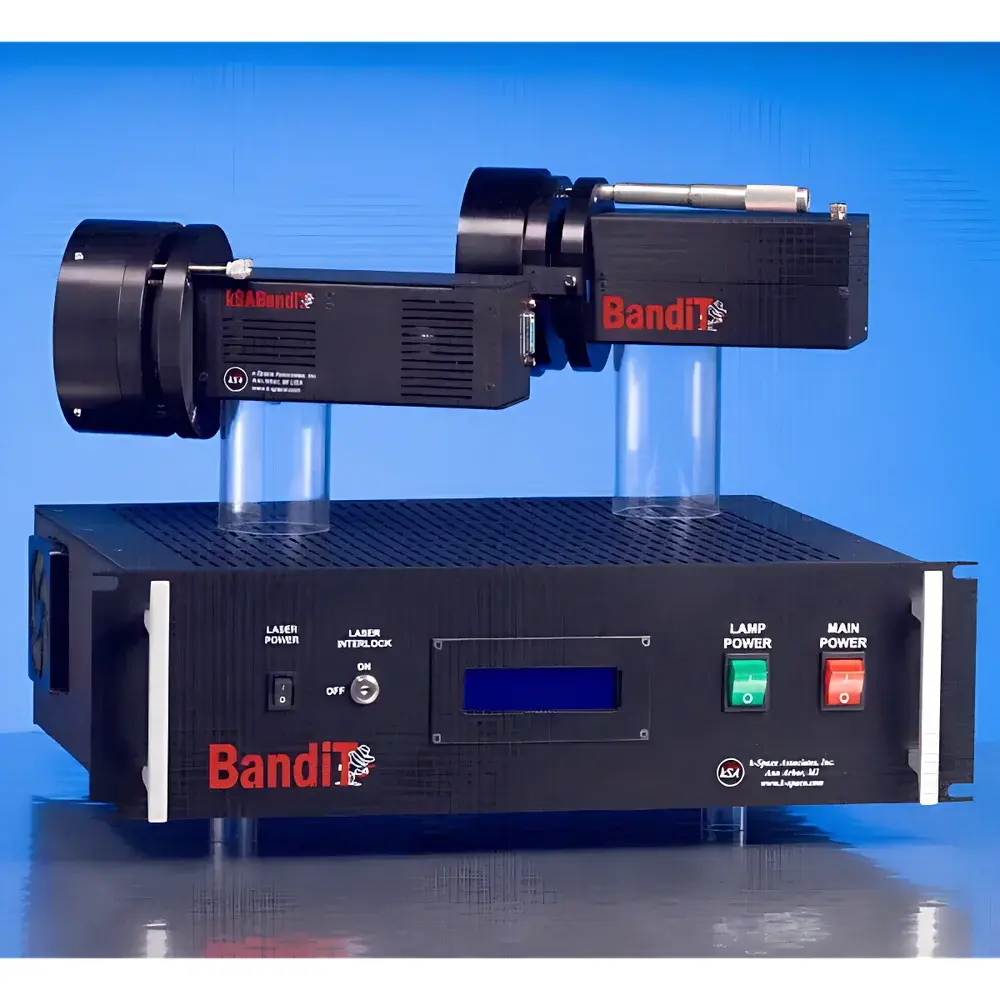
k-Space Associates kSA BandiT Real-Time Substrate Temperature Monitor
| Brand | k-Space Associates |
|---|---|
| Model | kSA BandiT |
| Origin | USA |
| Type | Non-Contact, Absorption-Edge-Based In-Situ Temperature Monitoring System for Semiconductor Wafers |
| Temperature Range | RT to 750 °C (up to 1300 °C with optional configuration) |
| Repeatability | ±0.2 °C |
| Resolution | 0.1 °C |
| Stability | ±0.2 °C |
| Measurement Principle | Temperature-Dependent Bandgap Absorption Edge Shift (Tauc Plot Method) |
| Compatible Platforms | MBE, MOCVD, Sputtering, PLD, Evaporation, Annealing & Rapid Thermal Processing (RTP) Systems |
| Laser Wavelength Options | Visible (e.g., 405 nm, 635 nm) and Near-IR (e.g., 980 nm, 1310 nm) |
| Surface Analysis Capabilities | In-situ deposition rate, film thickness estimation, and surface roughness correlation |
| Optical Interface | Standard viewport-compatible |
| Software | kSA BandiT Multi-Wafer Mapping Suite with motorized XY scanning stage control |
Overview
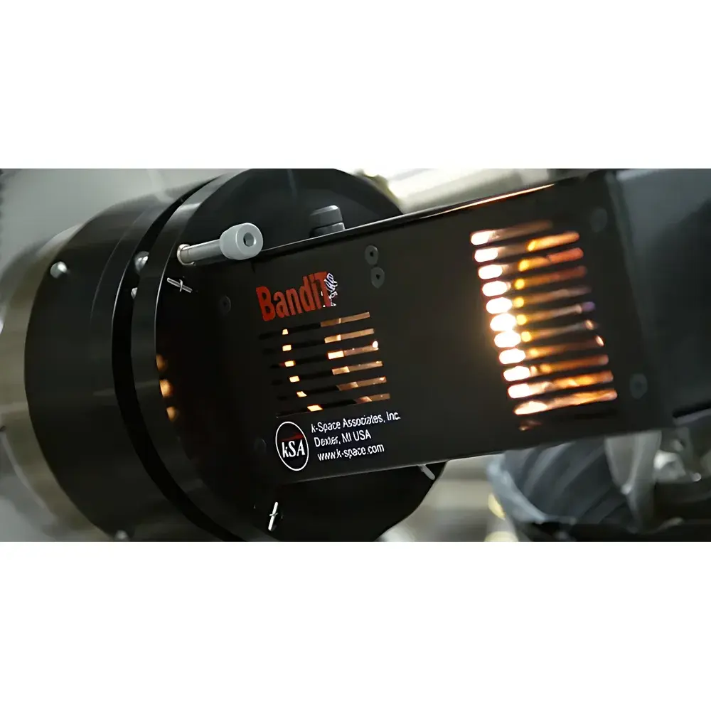
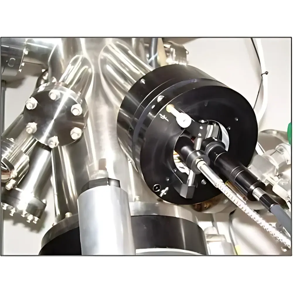
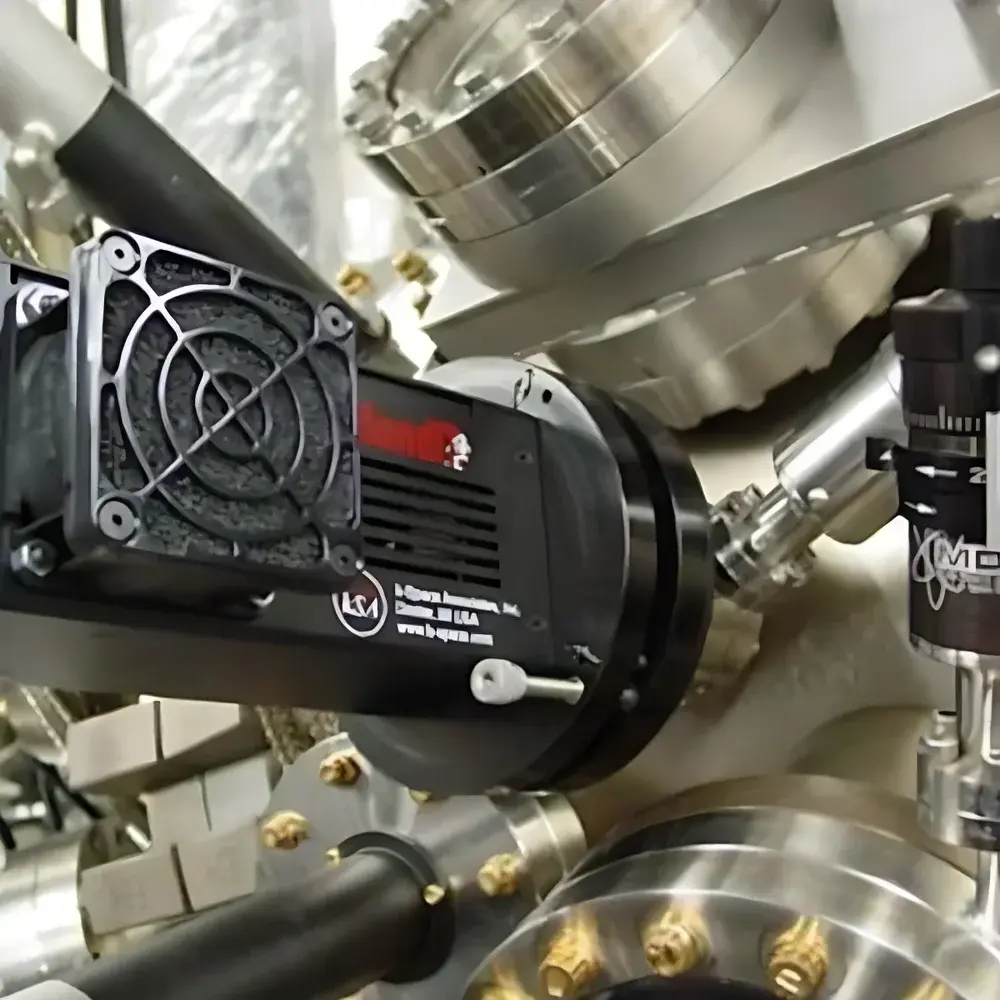
The k-Space Associates kSA BandiT Real-Time Substrate Temperature Monitor is an in-situ, non-contact optical diagnostic system engineered for precision temperature measurement of semiconductor wafers and substrates during thin-film growth and thermal processing. Unlike conventional pyrometry—whose accuracy is compromised by emissivity uncertainty—the kSA BandiT leverages the fundamental semiconductor property that the absorption edge (bandgap energy) shifts predictably with temperature. By monitoring spectral changes in reflected or transmitted light near the material’s band edge, the system calculates absolute surface temperature directly from first principles, independent of surface emissivity, oxidation state, or film coverage. This physics-based approach ensures traceable, repeatable, and calibration-stable measurements across diverse substrate materials—including Si, GaAs, InP, GaN, SiC, and transition metal dichalcogenides—under ultra-high vacuum (UHV), low-pressure, or atmospheric conditions. The system is routinely integrated into molecular beam epitaxy (MBE), metalorganic chemical vapor deposition (MOCVD), pulsed laser deposition (PLD), sputtering, and rapid thermal annealing (RTA) platforms, where real-time thermal uniformity is critical to stoichiometry control, interface sharpness, and defect suppression.
Key Features
- True non-contact, non-invasive measurement—no thermal perturbation or sensor loading on the wafer
- Direct bandgap-derived temperature quantification eliminates emissivity-related drift common in broadband pyrometers
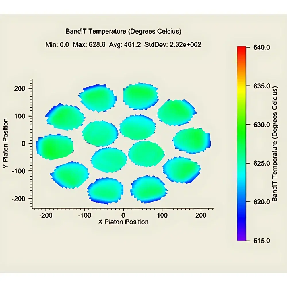
- Motorized XY scanning stage enables automated 2D temperature mapping across multi-wafer carriers or large-area substrates (up to 6-inch diameter)
- Multi-wavelength laser options support material-specific optimization: visible lasers for wide-bandgap semiconductors (e.g., GaN, ZnO); near-IR for Si and Ge
- Simultaneous acquisition of temperature, relative deposition rate (via reflectance oscillation analysis), and surface morphology indicators (via scattering signature trends)
- Robust optical design compatible with standard quartz or sapphire viewports—no specialized AR coatings required
- Real-time data streaming at up to 10 Hz per spatial point, synchronized with process controllers via TTL or Ethernet/IP
Sample Compatibility & Compliance
The kSA BandiT is validated for use with crystalline and polycrystalline semiconductor substrates ranging from 2-inch to 6-inch diameter, including bare wafers, epitaxial templates, and partially deposited heterostructures. It supports operation under UHV (<1×10⁻¹⁰ Torr), MOCVD reactor environments (up to 100 Torr), and ambient-pressure RTP furnaces. The system complies with ISO/IEC 17025 traceability requirements for optical metrology when used with NIST-traceable reference sources. Its firmware architecture supports audit-ready logging per FDA 21 CFR Part 11 guidelines, including electronic signatures, user access controls, and immutable timestamped records—making it suitable for GLP/GMP-regulated R&D and pilot-line manufacturing environments.
Software & Data Management
The kSA BandiT Control and Mapping Software provides a deterministic, scriptable interface built on LabVIEW RT and Python APIs. Users define custom scan patterns (raster, spiral, or user-defined ROI), set thermal alarm thresholds, and export time-resolved 2D temperature matrices in HDF5 or CSV formats. Integrated signal processing includes Savitzky-Golay filtering, baseline correction for window transmission drift, and real-time Tauc plot fitting using constrained nonlinear least-squares optimization. All raw spectra and derived parameters are stored with full metadata (chamber pressure, source shutter status, heater setpoint), enabling post-process correlation with XRD, AFM, or PL data. Remote monitoring and configuration are supported via secure HTTPS and SSH protocols.
Applications
- MBE growth optimization: Identifying radial and azimuthal thermal gradients affecting dopant incorporation and layer uniformity
- MOCVD reactor qualification: Verifying thermal profile stability during ramp-up, soak, and cooldown phases
- Sputter-deposited TCO characterization: Correlating substrate temperature with carrier mobility and optical bandgap in ITO or AZO films
- In-situ stress evolution monitoring: Detecting thermally induced lattice mismatch during heteroepitaxy via localized temperature deviation
- Process transfer validation: Benchmarking thermal behavior across tool generations or fab sites using identical band-edge calibration protocols
- Fundamental studies of phase transitions: Capturing nucleation onset temperatures in VO₂ or NiTi thin films during dynamic heating
FAQ
How does the kSA BandiT differ from conventional infrared pyrometers?
It measures temperature via the temperature-dependent shift of the semiconductor absorption edge—not blackbody radiation—making it immune to emissivity variation, surface contamination, or partial film coverage.
Can the system operate during active deposition?
Yes. Its high-speed spectral acquisition and narrow-band laser illumination enable continuous monitoring even under intense plasma or effusion cell fluxes.
Is calibration required between different wafer materials?
Each material requires an initial bandgap-vs-temperature reference curve (typically supplied by k-Space or measured in situ), but no recurring recalibration is needed under stable optical alignment.
What vacuum compatibility does the optical head provide?
The probe head is rated for UHV service (bakeable to 150 °C); fiber-coupled design isolates sensitive electronics from chamber environment.
Does the system support integration with third-party PLCs or recipe managers?
Yes—via Modbus TCP, EtherCAT, or custom OPC UA nodes, enabling closed-loop thermal feedback control in production tools.


