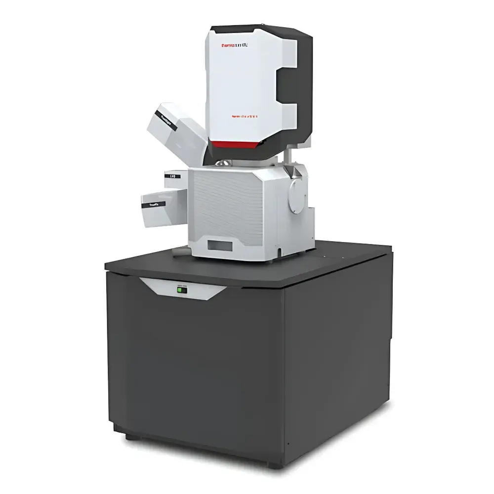
Thermo Fisher Scientific Apreo ChemiSEM Field Emission Scanning Electron Microscope
| Brand | Thermo Fisher Scientific |
|---|---|
| Origin | Czech Republic |
| Model | Apreo ChemiSEM |
| Instrument Type | Floor-standing High-Resolution FE-SEM |
| Electron Gun | Schottky Thermal Field Emission |
| Secondary Electron Resolution | 0.7 nm @ 30 kV |
| Backscattered Electron Resolution | 0.7 nm @ 30 kV |
| Magnification Range | 50× – 1,000,000× |
| Accelerating Voltage | 200 V – 30 kV |
| Landing Energy Range | 20 eV – 30 keV |
| Maximum Sample Size at 10 mm WD | 3 mm (min. mag. 29×) |
| Chamber Ports | 18 |
| Stage Travel | X = 110 mm, Y = 110 mm, Z = 65 mm, Tilt = −15° to +90°, Rotation = 360° continuous |
| Standard Detector System | Trinity In-lens Detection System (T1, T2, T3), TD, DBS |
| Optional Detectors | DBS-GAD, Low-Vacuum SE Detector, STEM 3+ Segmented Detector (BF/DF/HADF/HAADF), IR CCD, Thermo Scientific™ Nav-Cam™ Navigation Camera |
Overview
The Thermo Fisher Scientific Apreo ChemiSEM is a high-performance field emission scanning electron microscope engineered for simultaneous high-resolution imaging, elemental composition analysis, and crystallographic characterization. Built upon a robust Schottky thermal field emission electron optical column, the system delivers sub-nanometer resolution—0.7 nm at 30 kV in both secondary electron (SE) and backscattered electron (BSE) modes—and maintains exceptional beam stability across a wide landing energy range (20 eV–30 keV). Its integrated ChemiSEM technology enables real-time, algorithm-driven quantitative elemental mapping without requiring user intervention in contrast or threshold adjustments. Unlike conventional SEM-EDS workflows, ChemiSEM embeds spectral deconvolution, background subtraction, and stoichiometric phase identification directly into image acquisition—enabling automated, reproducible compositional analysis even for multi-phase industrial alloys, ceramics, or geological specimens. The system operates under fully oil-free vacuum conditions (<6.3 × 10⁻⁶ mbar after 12 h pump-down), with rapid evacuation (<3.5 min) and optional low-vacuum capability (10–500 Pa) for charge-sensitive or non-conductive samples.
Key Features
- Trinity In-lens Detection System: Three spatially segmented detectors (T1, T2, T3) positioned within the objective lens and column enable concurrent acquisition of topographic, atomic-number-contrast, and compositional signals—eliminating the need for sequential detector repositioning.
- ChemiSEM Technology Suite: Integrates TrueSight Pro EDS (25 or 70 mm² active area, 125 eV Mn Kα energy resolution), ChemiPhase multivariate statistical phase identification, and ChemiView offline data reprocessing—all unified under the xT SEM interface.
- TruePix EBSD Detector: Hybrid pixelated direct-electron detector with zero readout noise, 2000 FPS frame rate, and automatic pattern center calibration—supporting full crystallographic indexing (all 7 crystal systems, 11 Laue groups) and seamless integration with EDS maps.
- SmartAlign & Auto-Optimization: Fully automated lens alignment, stigmation correction, focus, and frame integration (SFI) reduce operator dependency and ensure consistent image quality across users and sessions.
- Electron Beam Deceleration (BD): Enables high-fidelity low-kV imaging (down to 500 V) with improved surface sensitivity and reduced charging on insulators—without external beam deceleration hardware.
- Modular Vacuum Architecture: Dual-stage turbomolecular pumping (240 L/s), ion getter pumps (IGP), and pressure-limiting apertures (PLA) support both ultra-high vacuum (UHV) and controlled low-vacuum operation.
Sample Compatibility & Compliance
The Apreo ChemiSEM accommodates diverse sample geometries—including bulk metals, polished cross-sections, wafers up to 200 mm diameter (with optional stage), and irregularly shaped industrial components—without mandatory size reduction. Its 110 mm × 110 mm × 65 mm XYZ travel range, ±90° tilt, and full 360° rotation support tilted-beam EBSD, serial sectioning, and tomographic workflows. The chamber features 18 standardized ports for detector expansion, gas injection systems (GIS), or in-situ heating/cooling stages. All analytical outputs comply with ISO/IEC 17025 requirements for testing laboratories; EDS quantification follows PROZA matrix correction protocols validated per ASTM E1508 and ISO 16700. Data integrity is maintained via audit-trail-enabled software adhering to FDA 21 CFR Part 11 principles—ensuring traceability of acquisition parameters, calibration events, and processing steps.
Software & Data Management
Control and analysis are unified within the 64-bit xT SEM platform running on Windows 10. Projects are stored hierarchically in a native database structure supporting versioned metadata, instrument configuration snapshots, and time-stamped acquisition logs. Quantitative EDS workflows include automatic peak identification, escape/sum peak removal, user-defined element inclusion/exclusion, and k-ratio-based or standardless (least-squares) quantification. ChemiSEM’s “always-on” mapping engine performs real-time spectrum stripping during acquisition, enabling immediate overlay of elemental distributions onto SE/BSE images. MAPS software integration supports automated montaging across multiple fields-of-view (FOVs), drift-corrected stitching (DCFII), and export to industry-standard formats (TIFF, JPEG, HDF5, .msa). EBSD data is processed using dedicated software featuring grain boundary detection, misorientation mapping, pole figure generation, and phase-specific orientation distribution functions (ODFs)—all exportable as CSV, XML, or CTF files compatible with third-party crystallography tools.
Applications
The Apreo ChemiSEM serves as a primary characterization tool in advanced materials R&D, metallurgy, semiconductor failure analysis, geosciences, and pharmaceutical solid-state analysis. In steel manufacturing, ChemiPhase identifies complex oxide/sulfide/nitride inclusions and calculates their volumetric fractions—critical for fatigue life prediction. In battery research, BD-mode imaging resolves SEI layer morphology on cycled electrodes at <1 kV, while simultaneous EDS/EBSD reveals Li-ion diffusion pathways correlated with grain orientation. For additive manufacturing, the system characterizes porosity distribution, melt pool boundaries, and residual stress-induced lattice distortions across multi-material builds. Its compatibility with CleanConnect™ sample transfer modules ensures contamination-free analysis of air-sensitive catalysts or organometallic compounds.
FAQ
What vacuum level is required for optimal EDS and EBSD performance?
High vacuum (<6.3 × 10⁻⁶ mbar) is mandatory for EDS spectral fidelity and EBSD pattern clarity; low-vacuum mode is restricted to SE imaging only.
Can the Apreo ChemiSEM perform automated particle analysis?
Yes—integrated MAPS software supports threshold-based particle segmentation, size distribution histograms, and composition-tagged classification across thousands of particles per map.
Is remote operation supported?
Full remote access is enabled via secure RDP or VNC protocols; all instrument controls, acquisition, and offline analysis functions remain fully functional.
How does SmartScan improve signal-to-noise ratio?
SmartScan applies adaptive dwell time modulation, line averaging, and frame integration—dynamically optimizing acquisition based on local signal intensity and beam stability.
What sample preparation standards does the system assume?
Standard conductive coating (e.g., Au/Pd sputtering) is recommended for non-conductive samples; however, low-kV BD imaging and charge compensation techniques minimize or eliminate the need for coating in many cases.


