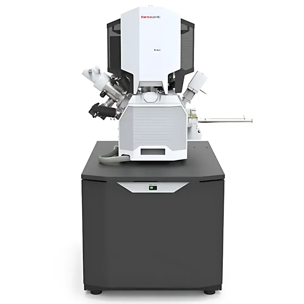
Thermo Fisher Scientific Scios 2 DualBeam Focused Ion Beam Scanning Electron Microscope
| Brand | Thermo Fisher Scientific |
|---|---|
| Origin | Czech Republic |
| Model | Scios 2 DualBeam |
| Electron Source | Schottky Field Emission Gun |
| STEM Resolution | 0.8 nm at 30 kV (WD = 7 mm) |
| SEM Resolution | 1.6 nm at 1 keV, 1.4 nm at 1 keV with beam deceleration |
| Ion Beam Resolution | 3.0 nm at 30 kV |
| Ion Beam Current Range | 1.5 pA – 65 nA |
| Electron Beam Current Range | 1 pA – 400 nA |
| Acceleration Voltage (e-beam) | 200 V – 30 kV |
| Landing Voltage (e-beam) | 20 eV – 30 kV |
| Acceleration Voltage (ion-beam) | 500 V – 30 kV |
| Stage | 5-axis motorized, X/Y = 110 mm, Z = 65 mm, tilt = −15° to +90°, rotation = 360° |
| Maximum Sample Diameter | 110 mm |
| Maximum Sample Height (at full X/Y rotation) | 85 mm |
| Maximum Sample Mass | 5 kg |
| Chamber Ports | 21 |
| Chamber Inner Width | 379 mm |
| Integrated Detectors | In-lens ETD, T1 (in-lens BSE), T2 (in-lens SE), optional T3 (in-lens SE), DBS (segmented solid-state BSE), ICE (ion conversion & electron detector), IR-CCD, Nav-Cam+™ optical navigation camera |
Overview
The Thermo Fisher Scientific Scios 2 DualBeam is a high-performance, ultra-high-resolution dual-beam system integrating a field-emission scanning electron microscope (FE-SEM) and a focused gallium ion beam (FIB) in a single, co-registered platform. Engineered for precision nanoscale characterization and site-specific sample preparation, the system leverages advanced electron and ion optics—including the NICol electron column and Sidewinder HT ion column—to deliver sub-nanometer imaging resolution and high-fidelity milling capability across diverse material classes. Its design addresses critical challenges in materials science, semiconductor metrology, life sciences, and geosciences, where non-conductive, magnetic, beam-sensitive, or heterogeneous specimens demand stable, low-voltage imaging, charge-compensated signal detection, and reproducible cross-sectional access. The Scios 2 operates under variable landing voltage conditions (down to 20 eV) and supports beam deceleration modes to minimize surface charging and subsurface damage—enabling reliable analysis of insulating ceramics, polymers, battery cathodes, and biological composites without conductive coating.
Key Features
- NICol Electron Column: Optimized for high-brightness, high-stability Schottky field emission, delivering <0.8 nm STEM resolution at 30 kV and 1.4 nm at 1 keV with beam deceleration—ideal for atomic-scale imaging and low-kV surface topography.
- Sidewinder HT Ion Column: High-current, high-resolution gallium FIB capable of 3.0 nm resolution at 30 kV and sustained beam stability over >1000 hours of source lifetime; enables rapid TEM lamella preparation, atom probe tip fabrication, and nanoscale circuit edit.
- Integrated Multi-Detector Architecture: Simultaneous acquisition from up to four detectors—including in-lens ETD (secondary electrons), T1/T2/T3 in-column SE/BSE, segmented DBS for compositional contrast, ICE for high-efficiency ion/electron signal separation, and IR-CCD for real-time stage height monitoring.
- Nav-Cam+™ Optical Navigation System: Integrated 5-megapixel color optical camera with automated montage stitching, enabling fast macro-to-nano correlation and precise region-of-interest (ROI) targeting prior to FIB milling or SEM imaging.
- SmartScan & DCFI Drift Compensation: Real-time beam scanning synchronization and active drift correction algorithms eliminate image artifacts during long-duration acquisitions or serial sectioning—critical for quantitative 3D tomography and time-resolved in situ experiments.
- MEMS Thermal Stage Integration: Fully compatible with Thermo Fisher’s high-speed, wide-range MEMS heating/cooling stages (−150°C to +1000°C), supporting dynamic in situ structural evolution studies under near-operational conditions.
Sample Compatibility & Compliance
The Scios 2 DualBeam accommodates a broad spectrum of specimen types—including bulk metals, oxides, layered 2D materials, porous frameworks, frozen-hydrated biological sections, and lithographically patterned wafers—without mandatory conductive coating. Its low-energy electron imaging mode (20 eV–5 keV), combined with charge-neutralization via flood gun and low-voltage BSE detection, ensures artifact-free imaging of insulators such as SiO₂, Al₂O₃, and polymer electrolytes. The system complies with ISO 16700:2016 (electron microscopy—terminology and definitions), ASTM E1558 (FIB sample preparation), and supports GLP/GMP-aligned workflows through audit-trail-enabled software logging. Optional ASV4 3D reconstruction software meets requirements for traceable volumetric data generation in R&D and failure analysis environments subject to internal quality protocols.
Software & Data Management
Controlled by the Thermo Scientific SmartEM platform, the Scios 2 provides a unified, customizable GUI with real-time quad-view display (up to four synchronized detector channels), scriptable automation (Python API), and native support for TIFF, DM3, and HDF5 export formats. Auto Slice & View 4 (ASV4) enables fully automated serial sectioning, alignment, and 3D reconstruction—including drift-corrected tilt-series acquisition and iterative tomographic reconstruction using SIRT or SART algorithms. All instrument parameters, user actions, and acquisition metadata are logged with timestamps and operator IDs—fully compliant with FDA 21 CFR Part 11 requirements when deployed with validated electronic signature modules. Raw data is stored on local RAID-protected storage or routed directly to network-attached storage (NAS) systems via GigE Vision and DICOM-compatible pipelines for enterprise-level integration.
Applications
- Materials Science: Quantitative grain boundary mapping in Ni-based superalloys, phase identification in multiphase battery electrodes (NMC/LFP/graphite), and strain-field analysis in strained-silicon heterostructures.
- Semiconductor Failure Analysis: Cross-sectional imaging of BEOL interconnects, trench depth profiling in EUV photoresists, and nanoscale defect isolation in FinFET devices using voltage-contrast FIB-SEM.
- Geosciences & Energy Materials: Pore-network quantification in shale matrix, solid-electrolyte interphase (SEI) layer thickness measurement in cycled Li-metal anodes, and catalyst nanoparticle dispersion analysis in PEM fuel cell membranes.
- Life Sciences: Correlative light-electron microscopy (CLEM) workflows using fiducial-based registration, cryo-FIB milling of vitrified cells for lamella-based cryo-ET, and serial block-face imaging of resin-embedded neural tissue.
- Additive Manufacturing: In-process defect characterization (lack-of-fusion pores, unmelted powder), residual stress mapping via crystallographic orientation contrast (EBSD integration), and fatigue crack initiation site localization.
FAQ
What is the minimum landing voltage supported for charge-sensitive samples?
The Scios 2 supports electron landing voltages as low as 20 eV, enabling high-fidelity imaging of uncoated insulators without charging artifacts.
Can the system perform automated TEM lamella preparation?
Yes—Auto Slice & View 4 software enables fully automated, recipe-driven lamella thinning, lift-out, and polishing with real-time endpoint detection via ion-induced secondary electron yield.
Is the system compatible with EBSD and EDS integration?
The Scios 2 chamber includes dedicated ports and mechanical interfaces for third-party EBSD detectors and silicon drift detectors (SDD), with synchronized acquisition and spatial calibration via SmartEM.
How is stage repeatability ensured during multi-step correlative workflows?
The 5-axis motorized stage achieves XY repeatability of ±3 µm and features hardware-encoded absolute positioning, enabling sub-micron repositioning accuracy across days-long experiments.
What vacuum specifications are required for optimal performance?
The electron column operates at ≤2×10⁻⁸ mbar, while the ion column maintains ≤5×10⁻⁷ mbar; differential pumping ensures independent pressure control and minimizes hydrocarbon contamination during extended FIB operation.


