3i HEMS & LT-AC/DC Hall Effect Measurement System
| Brand | 3i |
|---|---|
| Origin | Germany |
| Manufacturer Type | Authorized Distributor |
| Origin Category | Imported |
| Model | HEMS & LT-AC/DC |
| Pricing | Upon Request |
Overview
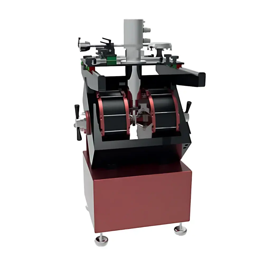
The 3i HEMS & LT-AC/DC Hall Effect Measurement System is a fully integrated, cryogenic-compatible platform engineered for precise electrical transport characterization of solid-state materials under controlled magnetic fields and temperature conditions. Based on the classical Hall effect and van der Pauw geometries, the system quantifies fundamental electronic parameters—including carrier concentration, mobility, resistivity, and sign of charge carriers—by applying orthogonal magnetic and electric fields while monitoring transverse voltage development. Its modular architecture supports both DC and AC measurement modes, enabling static Hall coefficient extraction as well as frequency-dependent impedance and AC susceptibility analysis. Designed for research-grade reproducibility, the system operates across an extended thermal range (1 K to 1273 K) and magnetic field range (up to 16 T with optional cryogenic magnet integration), making it suitable for advanced studies in semiconductor physics, oxide electronics, quantum transport, and emerging nanomaterials.
Key Features
- Multi-mode electrical transport capability: DC Hall/resistivity, AC resistance, AC susceptibility, and Shubnikov–de Haas oscillation analysis
- High-field compatibility: Up to 2.5 T standard; expandable to 16 T using external superconducting magnet and low-temperature insert
- Wide temperature coverage: 1 K–300 K (with cryostat); 3 K–1273 K (with high-temperature probe options)
- Precision probe positioning: Motorized XYZ stage with sub-micron repeatability and 12-point contact capability per sample
- Van der Pauw and 6-terminal Hall configurations supported via configurable wiring harnesses and shielded cabling
- Ultra-low-noise electronics: Voltage resolution down to 10 pV (DC), 100 nV (AC), and input noise floor of 1.5 nV/√Hz at 1 kHz
- Rotatable sample stage: 360° continuous rotation with 0.016° angular resolution for anisotropy mapping and field-angle-dependent measurements
- Standard vacuum interface: KF50 or KF40 flange compatibility for seamless integration into existing cryogenic or UHV systems
Sample Compatibility & Compliance
The system accommodates planar samples up to 10 mm × 10 mm (standard) or 5 mm × 10 mm (rotational insert), with customizable sample holders supporting up to 12 electrical contacts. Sample mounting utilizes gold-plated spring-loaded probes or lithographic contact pads compatible with standard microfabrication processes. All measurement protocols adhere to ASTM F76 (Standard Test Method for Measuring Resistivity of Semiconductor Materials) and ISO/IEC 17025 traceability requirements when operated with calibrated reference standards. Data acquisition and instrument control comply with GLP/GMP documentation frameworks, including full audit trail logging, user access controls, and electronic signature support per FDA 21 CFR Part 11 where configured.
Software & Data Management
The proprietary 3i Measurement Suite provides a unified GUI for experiment sequencing, real-time parameter monitoring, and post-acquisition analysis. It supports automated ramping of magnetic field, temperature, and current bias with synchronized data capture at user-defined intervals. Raw time-series and swept-parameter datasets are stored in HDF5 format with embedded metadata (field, temperature, current, timestamp, calibration coefficients). Built-in analysis modules include Hall coefficient derivation, mobility vs. temperature fitting, quantum oscillation FFT analysis, and complex impedance modeling (Z′ and Z″). Export options include CSV, MATLAB .mat, and Python-compatible NumPy arrays. Remote operation via TCP/IP and LabVIEW driver support enable integration into automated lab environments.
Applications
- Characterization of doped semiconductors (Si, GaAs, GaN, SiC) and 2D materials (graphene, TMDCs) for mobility-lifetime product evaluation
- Charge carrier dynamics in transition metal oxides (e.g., LaAlO₃/SrTiO₃ heterostructures) and organic conductors (PEDOT:PSS, pentacene derivatives)
- Quantum transport studies including Shubnikov–de Haas oscillations in GaInAs quantum wells and Landau level spectroscopy
- Thermoelectric material screening via simultaneous Seebeck coefficient and Hall mobility mapping
- Defect engineering validation in radiation-hardened space-grade electronics and high-power device substrates
- Process development feedback for epitaxial growth (MBE, MOCVD) and thin-film deposition (sputtering, ALD)
FAQ
What is the minimum detectable carrier concentration using this system?
The system achieves carrier concentration resolution down to ~1 × 10¹⁸ cm⁻³ under optimal signal-to-noise conditions (10 K, 1 T, 1 mA excitation), limited primarily by contact geometry and sample homogeneity.
Can the system perform simultaneous Hall and Seebeck measurements?
No—Seebeck coefficient measurement requires dedicated thermoelectric hardware (dual-thermocouple setup, thermal gradient control). However, the HEMS platform can be interfaced with third-party thermoelectric stages via analog I/O and synchronization triggers.
Is the software compatible with Windows 11 and 64-bit MATLAB R2022b or later?
Yes—the Measurement Suite is validated on Windows 10/11 (64-bit) and includes native MATLAB interface libraries compliant with R2022b through R2024a.
What vacuum level is required for low-temperature AC susceptibility measurements?
For optimal thermal stability below 4 K, a base pressure ≤5 × 10⁻⁶ mbar is recommended; AC susceptibility sensitivity degrades above 10⁻⁴ mbar due to residual gas conduction and eddy current interference.
Are calibration standards included with the system?
A NIST-traceable vanadium oxide (VO₂) reference sample and certified copper resistor standard are supplied for initial system verification and periodic recalibration.


