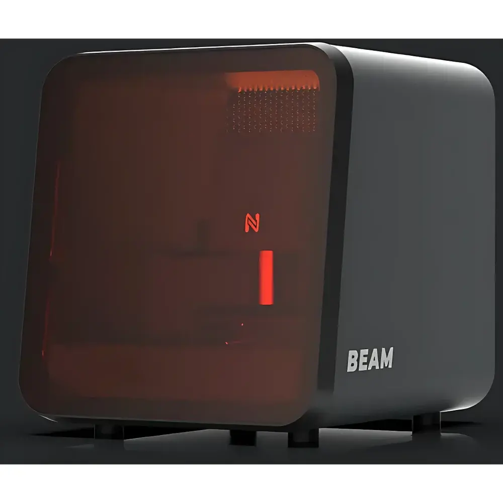
NILT BeamX Desktop Maskless Direct Write Lithography System
| Brand | NILT |
|---|---|
| Origin | Imported |
| Manufacturer Type | Authorized Distributor |
| Exposure Mode | Proximity |
| Resolution | 500 nm |
| Light Source | UV Laser |
| Wavelengths | 405 nm, 365 nm, 385 nm |
| Illumination Uniformity | Direct-write scanning mode |
| Maximum Exposure Area | 150 mm × 150 mm |
| Compatible Substrate Sizes | Up to 6-inch wafers |
| Autofocus Speed | <1 s (piezo-driven closed-loop optical focus control) |
| Pattern Writing Speed | <2 s per defined exposure field |
| Alignment Method | Semi-automated multi-layer alignment with real-time image recognition |
| Software Interface | GDSII-compatible, CNC-style navigation (WASD), on-the-fly pattern placement, wafer-level map visualization |
Overview
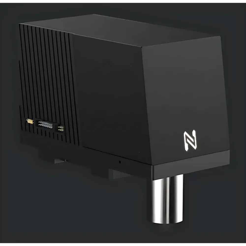
The NILT BeamX Desktop Maskless Direct Write Lithography System is an engineered solution for high-resolution, mask-free micro- and nanofabrication in academic laboratories, R&D centers, and low-volume semiconductor prototyping environments. Unlike conventional photolithography tools requiring physical photomasks, the BeamX employs a digitally controlled UV laser beam—focused to its diffraction limit—to directly expose photoresist-coated substrates via precision vector scanning. This direct-write approach eliminates mask fabrication costs and lead times while enabling rapid iteration of design layouts. The system operates on the principle of localized photochemical reaction induction: when the 365 nm, 385 nm, or 405 nm UV laser spot interacts with standard positive or negative resists (e.g., AZ5214E), it triggers solubility changes confined to sub-500 nm feature dimensions. Its compact footprint integrates a high-stability optical engine, piezo-actuated autofocus module, motorized XY stage, and real-time vision-based alignment subsystem—enabling reliable patterning across silicon wafers, glass, quartz, and polymer substrates up to 150 mm × 150 mm.
Key Features
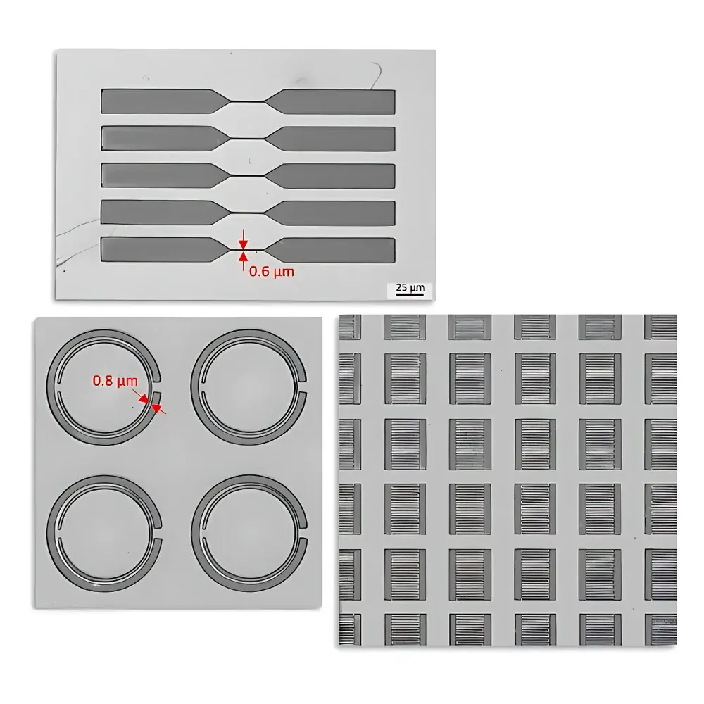
- Sub-500 nm resolution capability verified on 6-inch silicon wafers using standard i-line compatible resists
- Multi-wavelength UV laser source (365/385/405 nm) optimized for broad resist compatibility and process flexibility
- Real-time closed-loop autofocus system with <1 s settling time, utilizing piezoelectric actuation and interferometric feedback
- CNC-style intuitive software interface with WASD keyboard navigation, context-sensitive right-click positioning, and GDSII file import
- Semi-automated multi-layer alignment supported by live camera feed and template-matching algorithms—achievable in under 3 minutes per layer
- Modular exposure field stitching architecture for seamless patterning across large-area substrates without mechanical drift compensation overhead
- Integrated wafer-level map viewer with zoomable GDS thumbnail navigation for precise region targeting
Sample Compatibility & Compliance
The BeamX accommodates rigid and semi-rigid substrates including Si, SiO₂/Si, fused silica, sapphire, and SU-8-coated PET. It supports standard lithographic processes compliant with ISO 14644-1 Class 5 cleanroom requirements when operated in controlled environments. While not certified for full production-line GMP compliance, the system meets essential traceability criteria for research-grade GLP documentation: all exposure parameters (laser power, dwell time, scan velocity, focus offset) are logged with timestamps and user identifiers. Export configurations include optional audit trail modules aligned with FDA 21 CFR Part 11 requirements for electronic records and signatures. Resist compatibility has been validated against common formulations referenced in ASTM D5239 (photoresist sensitivity testing) and ISO 10788 (lithographic process characterization).
Software & Data Management
The BeamX Control Suite runs on Windows OS and provides native support for industry-standard GDSII and OASIS layout formats. All pattern data is stored in encrypted SQLite databases with versioned backups. The software enforces role-based access control (RBAC) for multi-user labs and maintains immutable logs of every exposure event—including machine state, environmental sensor readings (optional ambient temperature/humidity monitoring), and operator credentials. Batch processing scripts can be scheduled via Python API integration, enabling automated multi-wafer runs with inter-run parameter validation. Data export options include CSV metadata reports, TIFF-aligned overlay images, and PDF-certified exposure certificates suitable for internal QA review or external collaboration handoffs.
Applications
The BeamX serves as a versatile platform across multiple advanced technology domains. In photonics, it fabricates photonic crystals, ridge waveguides, microlens arrays, and diffractive optical elements (DOEs) for integrated optical interconnects and computational imaging systems. In biomedicine, it structures PDMS molds for microfluidic chips, generates topographical cues on tissue engineering scaffolds, and patterns electrode arrays for electrochemical biosensors. In microelectronics, it enables rapid prototyping of MEMS devices (e.g., cantilevers, resonators, actuators), RF components (IDTs, asymmetric open-ring resonators), and hybrid IC test structures—particularly where mask cost or turnaround time prohibits traditional fabrication routes. Its ability to write arbitrary text, logos, or fiducial markers directly onto resist layers further supports device identification, calibration artifact generation, and educational demonstration workflows.
FAQ
What resist types are compatible with the BeamX system?
Standard i-line and g-line positive resists (e.g., AZ5214E, S1813, ma-N 2401) and negative resists (e.g., SU-8 2000 series) have been characterized for use with 365–405 nm exposure. Resists must be spin-coated and soft-baked per manufacturer specifications.
Does the system support alignment to pre-existing features on a substrate?
Yes—via real-time optical recognition of alignment marks (crosses, squares, or custom shapes) using integrated CMOS imaging. Sub-pixel registration accuracy is maintained through iterative correlation matching and stage correction.
Can the BeamX perform grayscale lithography?
No—it operates in binary exposure mode only. Grayscale patterning requires modulated dose control not implemented in this configuration.
Is vacuum or nitrogen purge required during operation?
Not required. The system operates stably in ambient air; however, inert atmosphere chambers can be integrated as an optional accessory for oxygen-sensitive resists.
What maintenance is recommended for long-term optical performance?
Quarterly inspection of objective lens cleanliness and annual recalibration of laser power meter and stage encoders are advised. NILT provides certified service contracts with remote diagnostics support.


