High-Resolution Nanoimprint Lithography (NIL) Templates
| Origin | Jiangsu, China |
|---|---|
| Manufacturer Type | Authorized Distributor |
| Origin Category | Domestic |
| Model Variants | Quartz / Silicon / Polymer Templates |
| Pricing | Available Upon Request |
| Template Materials | Fused Silica (Quartz), Single-Crystal Silicon, Silicon Nitride (SiNₓ), Silicon Carbide (SiC), Borosilicate Glass |
| Max Template Diameter | 100 mm (4″) |
| Minimum Feature Size | 50 nm (for ≤2″ area) |
| EBL Service Capability | Down to 30 nm feature size |
| Substrate Compatibility | Conductive (e.g., Si, GaAs, InP) and Non-Conductive (e.g., SiO₂/Si, quartz, polymer-coated wafers) substrates |
| Fabrication Scope | Micro- and nanoscale patterning on Si, III–V (GaAs, InP), II–VI (ZnS, CdTe), and polymer substrates |
Overview
High-resolution nanoimprint lithography (NIL) templates are precision-engineered master stamps used to transfer nanoscale patterns onto functional substrates via mechanical deformation—either thermally induced (thermal NIL) or UV-curable resist-based (UV-NIL). Unlike conventional photolithography, NIL achieves sub-50 nm resolution without optical diffraction limits, making it a critical enabling technology for advanced semiconductor packaging, photonics, metasurfaces, and high-density data storage. These templates are fabricated using electron beam lithography (EBL) followed by reactive ion etching (RIE) or ion beam milling, ensuring atomic-level fidelity, low line-edge roughness (<1.5 nm RMS), and long-term mechanical stability under repeated imprint cycles. Designed for compatibility with industry-standard NIL platforms—including Obducat Eitre series, SUSS MicroTec MA/BA systems, EVG620/720 imprint tools, and Canon’s FPA-1200NZ2C—the templates support both rigid and soft imprint modalities across wafer diameters up to 100 mm (4″).
Key Features
- Multi-material platform: Selectable base substrates include fused silica (quartz) for UV transparency and thermal stability, single-crystal silicon for high stiffness and etch durability, silicon nitride for chemical inertness in aggressive developers, and polymeric variants (e.g., PDMS, OrmoStamp) for conformal contact on non-planar surfaces.
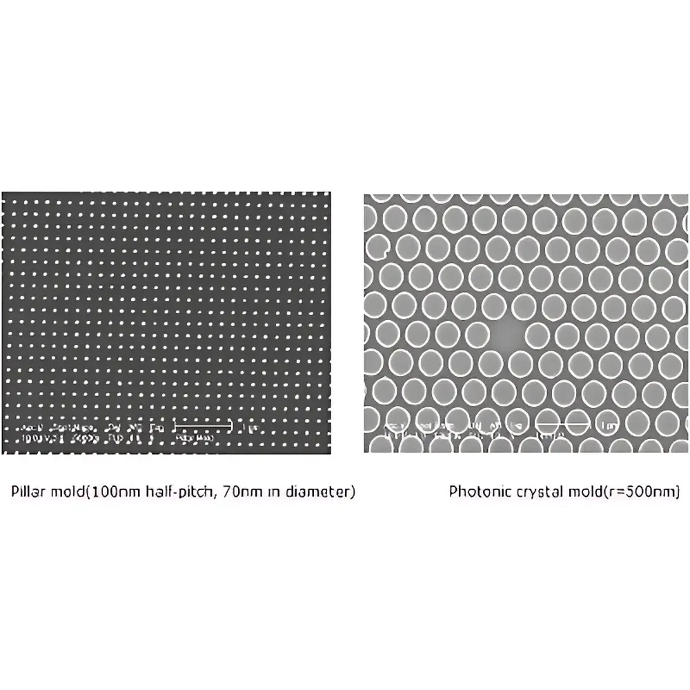
- Scalable resolution architecture: Full-wafer (4″) templates maintain ≤100 nm half-pitch features; reduced-area masks (≤2″) achieve ≤50 nm critical dimensions—validated by CD-SEM metrology traceable to NIST standards.
- Curved-surface compatibility: Soft polymer templates enable conformal imprinting on spherical, cylindrical, or freeform substrates—eliminating the need for custom vacuum chuck design or adaptive alignment optics.
- EBL service integration: On-demand pattern generation supports arbitrary layouts (gratings, photonic crystals, plasmonic arrays, bio-sensor motifs) with ≤30 nm minimum feature size, registered to substrate fiducials with <±25 nm overlay accuracy.
- Process-hardened surface finish: All rigid templates undergo anti-sticking coating (e.g., fluorinated self-assembled monolayers) and optional DLC (diamond-like carbon) hardening to extend lifetime beyond 500 imprint cycles without measurable CD drift.
Sample Compatibility & Compliance
Templates accommodate standard semiconductor wafers (Si, GaAs, InP, sapphire, quartz, SOI) and flexible substrates (PET, PI, glass slides) across thicknesses from 100 µm to 1 mm. Each batch is supplied with full QC documentation, including AFM topography maps, CD-SEM cross-sections, and reflectance/transmission spectra (190–1100 nm). Manufacturing adheres to ISO 9001:2015 quality management protocols. For regulated environments (e.g., compound semiconductor fabs or photonics R&D labs operating under GLP/GMP), traceability includes lot-specific calibration certificates and material safety data sheets (MSDS) compliant with REACH and RoHS directives.
Software & Data Management
No embedded firmware or proprietary software is required—templates operate as passive physical masters within host NIL equipment. However, digital design files (GDSII/OASIS) are delivered with each order and fully compatible with industry-standard mask data preparation (MDP) flows (e.g., Mentor Calibre, Cadence Pegasus). Optional services include DRC/LVS validation reports, OPC-free layout verification, and secure cloud-based file sharing with AES-256 encryption. Audit trails for EBL job parameters (beam current, dwell time, stage velocity) are retained for 7 years per internal SOPs aligned with FDA 21 CFR Part 11 principles for electronic records.
Applications
- High-throughput fabrication of sub-wavelength optical elements (metalenses, diffractive waveguides) for AR/VR and LiDAR systems
- Nanopatterning of plasmonic biosensor chips with reproducible SERS enhancement factors >10⁷
- Manufacturing of nanostructured anti-reflective and superhydrophobic coatings for solar cells and display optics
- Direct-write replication of quantum dot arrays and photonic bandgap structures in III–V heteroepitaxial stacks
- Rapid prototyping of microfluidic master molds for PDMS casting in organ-on-chip platforms
FAQ
What materials are available for rigid NIL templates?
Fused silica (quartz), single-crystal silicon, silicon nitride (SiNx), silicon carbide (SiC), and borosilicate glass—all polished to λ/10 surface flatness and coated with anti-adhesion layers.
Can you fabricate templates for non-circular substrates?
Yes—we support rectangular, elliptical, and custom-shaped substrates up to 100 × 100 mm², with edge exclusion zones defined per customer specification.
Is EBL pattern data validated before template fabrication?
All GDSII/OASIS files undergo automated DRC checking (minimum spacing, width, enclosure rules) and manual layout review by our process engineers prior to exposure.
Do you provide lifetime testing data for repeated imprint cycles?
Yes—accelerated wear testing (500+ cycles at 120 °C, 10 bar pressure) is performed on representative lots, with post-cycle CD metrology and defect density reporting included in QC packets.
Are templates compatible with hybrid lithography processes (e.g., NIL + etch transfer)?
Absolutely—templates are optimized for high-fidelity resist replication prior to plasma etch (ICP-RIE, Bosch process) or lift-off, with sidewall verticality >88° and aspect ratios up to 10:1 demonstrated on Si and GaN substrates.


