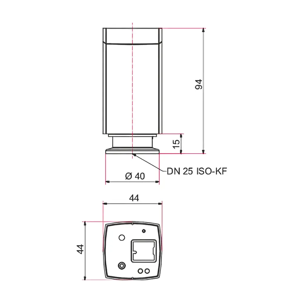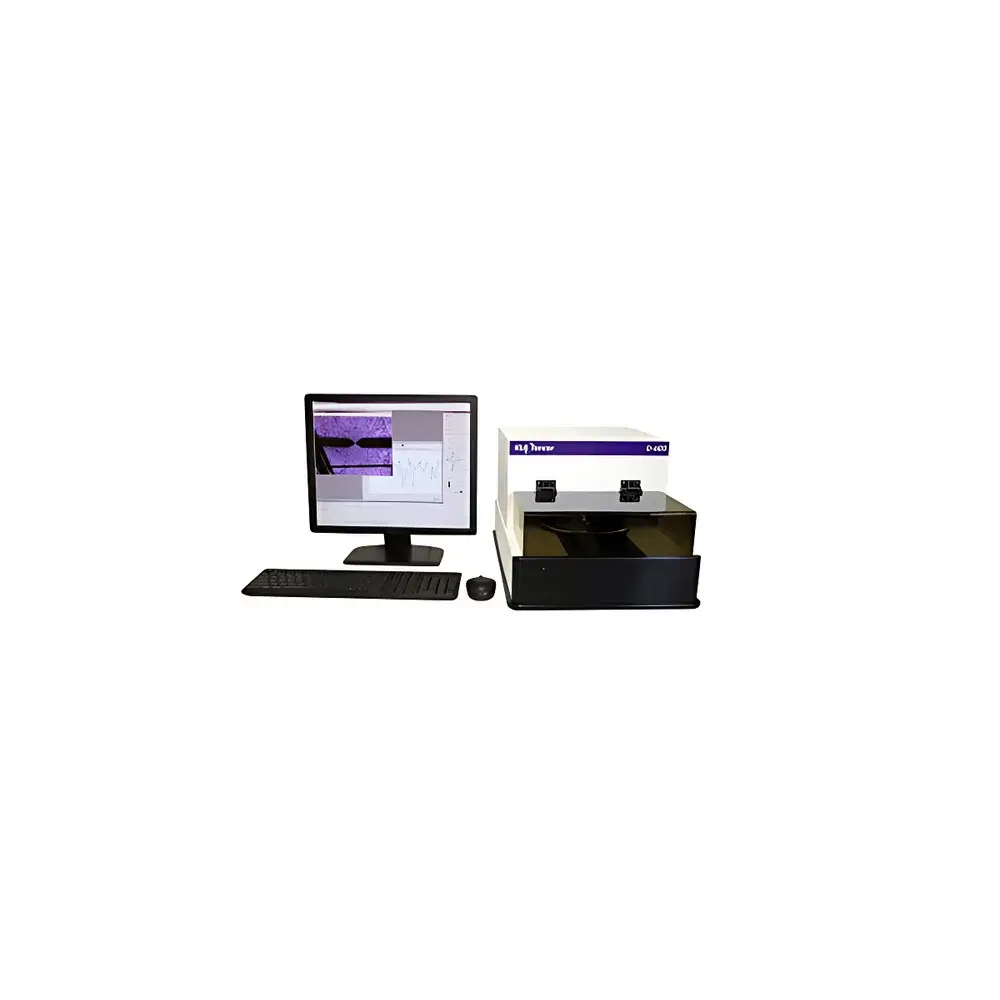
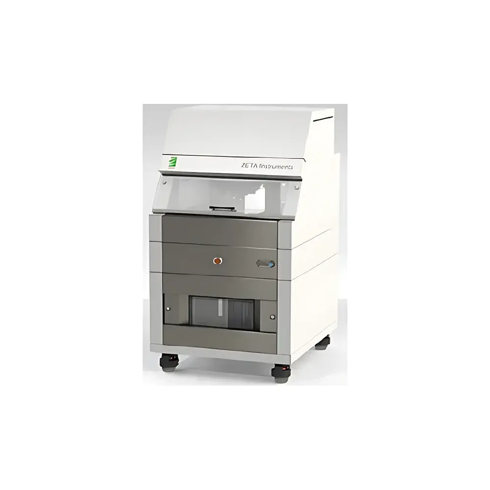
Keysight D.T Advanced Profilometer / Optical Surface Profilometer
| Brand | Keysight |
|---|---|
| Origin | Malaysia |
| Manufacturer Type | Authorized Distributor |
| Import Status | Imported |
| Model | D.T |
| Measurement Range | 5 nm – 1200 µm |
| Accuracy | ±1% |
| Probe Tip Radius | 2 µm |
| Normal Force | 1–15 mg |
| Scan Length | 55 µm |
| Step Height Repeatability | <4 Å |
| Vertical Resolution | 1 Å |
| Maximum Sample Size | 200 mm |
Overview
The Keysight D.T Advanced Profilometer is a high-precision, contact-mode surface metrology instrument engineered for nanoscale step height, topographic, and thin-film stress characterization. Leveraging a calibrated stylus-based scanning principle—rooted in established ISO 25178-2 and ASTM E1316 standards—the system delivers traceable vertical measurements across an exceptionally broad dynamic range (5 nm to 1200 µm) with sub-angstrom resolution. Unlike optical interferometric or confocal methods, the D.T employs a mechanically scanned diamond-tipped probe operating under precisely controlled normal force (1–15 mg), enabling quantitative profiling of both reflective and non-reflective surfaces—including rough metals, patterned semiconductors, MEMS structures, and coated optical components—without reliance on optical contrast or coherence length limitations.
Key Features
- Sub-ångström vertical resolution (1 Å) verified via NIST-traceable calibration artifacts, supporting critical applications in semiconductor process control and advanced packaging metrology.
- Z-axis measurement range spanning three orders of magnitude—from atomic-scale steps (5 nm) to macroscopic features (1200 µm)—eliminating the need for multiple instruments across R&D and production environments.
- Programmable probe force control (1–15 mg) ensures consistent tip-sample interaction across diverse material classes (e.g., soft polymers, hard ceramics, brittle oxides), minimizing ploughing or deformation artifacts.
- 2 µm probe tip radius optimized for high-fidelity edge detection and accurate step height quantification on lithographically defined features down to sub-micron linewidths.
- Integrated motorized XY stage accommodates wafers and substrates up to 200 mm diameter, with automated alignment routines for repeatable positioning within ±0.5 µm lateral accuracy.
- Rugged mechanical architecture with active vibration isolation and thermal drift compensation (<0.05 nm/°C), enabling stable long-duration scans in standard lab environments without dedicated cleanroom infrastructure.
Sample Compatibility & Compliance
The D.T profilometer supports direct measurement of conductive and non-conductive samples—including silicon wafers, glass substrates, sputtered metal films, spin-coated photoresists, and biomedical coatings—without conductive coating or vacuum requirements. Its mechanical sensing modality complies with ISO 25178-601 (areal surface texture) and ISO 4287 (profile-based roughness), and meets key requirements for GLP/GMP-regulated environments when paired with optional audit trail and electronic signature modules (21 CFR Part 11 compliant). Data export formats include ASCII, CSV, and ISO-standard .x3p files for interoperability with third-party analysis platforms such as MountainsMap® and Gwyddion.
Software & Data Management
The instrument operates under Keysight’s Profilometer Control Suite v5.x—a Windows-based application providing real-time scan monitoring, multi-point referencing, and automated feature extraction (e.g., step height, slope angle, curvature radius, film thickness via multi-scan differential analysis). All measurement sessions are timestamped and logged with full parameter metadata; optional software modules enable automated report generation per ISO/IEC 17025 templates, statistical process control (SPC) charting, and integration with enterprise LIMS systems via OPC UA or RESTful API. Raw data retention, user access controls, and revision history tracking satisfy FDA and EU Annex 11 documentation integrity requirements.
Applications
- Semiconductor: Quantifying etch depth, CMP uniformity, gate stack step coverage, and TSV sidewall profiles.
- MEMS/NEMS: Measuring released structure deflection, residual stress-induced bow, and release etch undercut.
- Optics & Photonics: Characterizing anti-reflective coating thickness gradients, diffractive optical element (DOE) groove depth, and laser mirror substrate flatness.
- Materials Science: Assessing thin-film adhesion failure morphology, corrosion pit depth distribution, and additive manufacturing layer interface fidelity.
- Quality Assurance Labs: Validating supplier wafer specifications against JEDEC JESD22-A108 (stress testing) and SEMI MF1530 (step height metrology).
FAQ
Is the D.T compatible with ISO 25178-compliant surface texture analysis?
Yes—the system acquires areal datasets meeting ISO 25178-2 profile acquisition criteria and exports native .x3p files for certified analysis in accredited software.
Can it measure steep sidewalls or high-aspect-ratio features?
With a 2 µm tip radius and programmable lateral approach angle, the D.T resolves slopes up to 75°; for >85° geometries, complementary AFM or CD-SEM is recommended.
What calibration standards are supplied with the instrument?
Keysight provides NIST-traceable step height reference artifacts (10 nm, 100 nm, 1 µm, and 10 µm certified steps) with full uncertainty budgets and recalibration services every 12 months.
Does the system support automated batch measurement of multiple sites?
Yes—via scriptable macros and coordinate-based site mapping, enabling unattended multi-wafer runs with pass/fail threshold reporting aligned to internal SPC limits.
Is remote diagnostics and firmware update supported?
All units include embedded Ethernet connectivity and TLS-secured remote access for Keysight Field Application Engineers, with over-the-air firmware updates validated per IEC 62443-3-3 cybersecurity guidelines.