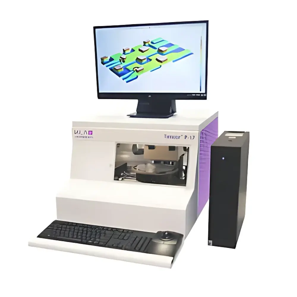
KLA P-17 Contact Profilometer
| Brand | KLA |
|---|---|
| Origin | Malaysia |
| Model | P-17 |
| Product Type | Contact Profilometer / Surface Roughness Tester |
| Operating Principle | Stylus-Based Profilometry |
| Scan Range | Up to 200 mm (no image stitching required) |
| Step Height Range | 1 nm to 1000 µm |
| Stylus Force Control | 0.03–50 mg |
| Camera Resolution | 5 MP color, optical zoom |
| Compliance | SEMI E4, E5, E30, E37 |
| Software Platform | Apex Analysis Software (ISO/ASME-compliant), Offline Analysis Module, SECS/GEM & HSMS support |
Overview
The KLA P-17 Contact Profilometer is the eighth-generation benchtop stylus-based surface metrology system engineered for high-precision, repeatable 2D and 3D topographic characterization in semiconductor fabrication, advanced packaging, MEMS development, and academic research environments. Utilizing a mechanical contact measurement principle—where a diamond-tipped stylus traverses the sample surface while sensing vertical displacement—the P-17 delivers traceable, quantitative data on step height, surface roughness, waviness, wafer bow, and thin-film stress. Its core architecture integrates an UltraLite® sensor with closed-loop force feedback, a vibration-isolated granite base, and a kinematically mounted, ultra-flat scanning stage capable of full-diameter measurements up to 200 mm without image tiling or stitching artifacts. Designed for both R&D validation and high-mix production floor deployment, the P-17 meets stringent requirements for GLP-compliant documentation, audit-ready data integrity, and seamless integration into automated fab environments via industry-standard communication protocols.
Key Features
- Stylus force control from 0.03 mg to 50 mg with real-time dynamic adjustment—enabling stable, non-destructive profiling of soft photoresists, polymer films, and fragile nanostructures.
- Full-wafer scanning capability: single-pass 200 mm linear scan range with sub-nanometer vertical resolution and <±0.2% step height repeatability (1σ) over 30-day calibration intervals.
- Integrated 5-megapixel color camera with optical zoom and dual-axis (top-view + side-view) illumination—supporting rapid feature identification, manual alignment, and automated pattern recognition.
- Real-time arc correction algorithm compensates for stylus trajectory curvature, eliminating systematic errors in high-aspect-ratio step measurements.
- Modular probe library: diamond stylus tips with radii from 40 nm to 50 µm and included angles from 20° to 100°—optimized for resolution vs. aspect ratio trade-offs across applications including TSV metrology and CMP endpoint verification.
- Apex software platform with ISO 4287/4288, ASME B46.1, and ISO 25178-2 compliant analysis modules—including leveling, Gaussian/Rational filtering, motif analysis, and Stoney equation-based stress calculation.
Sample Compatibility & Compliance
The P-17 accommodates substrates from 50 mm to 200 mm in diameter using a vacuum chuck with precision locating pins; optional carriers support 300 mm wafers (P-17 OF variant), solar panels (up to 240 × 240 mm), and HDD platters. For stress measurement, the three-point support stage ensures accurate bow quantification per ASTM F390 and SEMI MF-1530. All hardware and firmware comply with SEMI standards E4 (SECS-II), E5 (GEM), E30 (equipment communications), and E37 (HSMS). Data handling adheres to FDA 21 CFR Part 11 requirements when configured with Apex’s electronic signature and audit trail functionality—ensuring regulatory readiness for medical device and pharmaceutical manufacturing QA/QC labs.
Software & Data Management
Apex Analysis Software serves as the unified interface for measurement setup, acquisition, post-processing, and reporting. It supports multilingual UI (11 languages), customizable pass/fail criteria, embedded annotation tools, and automated report generation in PDF, CSV, and XML formats. Offline Analysis Software replicates all acquisition and analysis capabilities—allowing engineers to develop recipes, validate algorithms, and reprocess historical datasets without instrument downtime. KLARF file import enables defect-driven metrology workflows: coordinates from inspection tools trigger automated repositioning and localized 2D/3D profiling. Full SECS/GEM implementation permits host-directed job queuing, parameter synchronization, and SPC data streaming to factory MES systems.
Applications
- Step Height Metrology: Quantifies film thickness in etch, deposition, spin-coating, and CMP processes—from atomic-layer ALD stacks (<1 nm) to thick electroplated copper bumps (up to 1000 µm).
- Roughness & Waviness Analysis: Separates short-wavelength roughness (Rq, Ra) from long-wavelength form errors (Wq, Wa) using configurable Gaussian or spline filters per ISO 16610.
- Wafer Bow & Global Shape: Measures full-surface topography to extract principal curvatures, radius of curvature, and Z-height deviations—critical for lithography overlay control and bonding alignment.
- Thin-Film Stress Mapping: Computes 2D stress distribution via Stoney’s equation applied to bow measurements before/after deposition; 3D stress reconstruction enabled by rotational multi-scan acquisition.
- Defect Morphology Characterization: Profiles scratch depth, particle height, and etch pit geometry directly from KLARF-defined coordinates—supporting root-cause analysis in yield enhancement programs.
FAQ
What is the minimum measurable step height with the P-17?
The system achieves sub-nanometer vertical resolution (≤0.1 nm RMS noise) and can reliably quantify steps as low as 1 nm using optimized low-force scanning and high-gain UltraLite® sensing.
Does the P-17 support NIST-traceable calibration?
Yes—VLSI Standards NIST-traceable step height reference wafers (8 nm to 250 µm oxide or Cr-on-quartz) are recommended for daily verification and quarterly recalibration.
Can the P-17 measure 300 mm wafers?
Standard P-17 configuration supports up to 200 mm; the P-17 OF (Open Frame) variant is available with extended stage travel and 300 mm compatibility.
Is Apex software validated for regulated environments?
Apex includes 21 CFR Part 11-compliant features—electronic signatures, role-based access control, immutable audit trails, and secure data export—validated per IQ/OQ protocols upon customer request.
How does the system handle warped or non-planar samples?
The three-point kinematic chuck and automated leveling routines compensate for substrate tilt and curvature; software-based polynomial or spline leveling removes global form prior to local feature analysis.