
Process Measurement & Detection Equipment
Filter
Showing 31–60 of 83 results
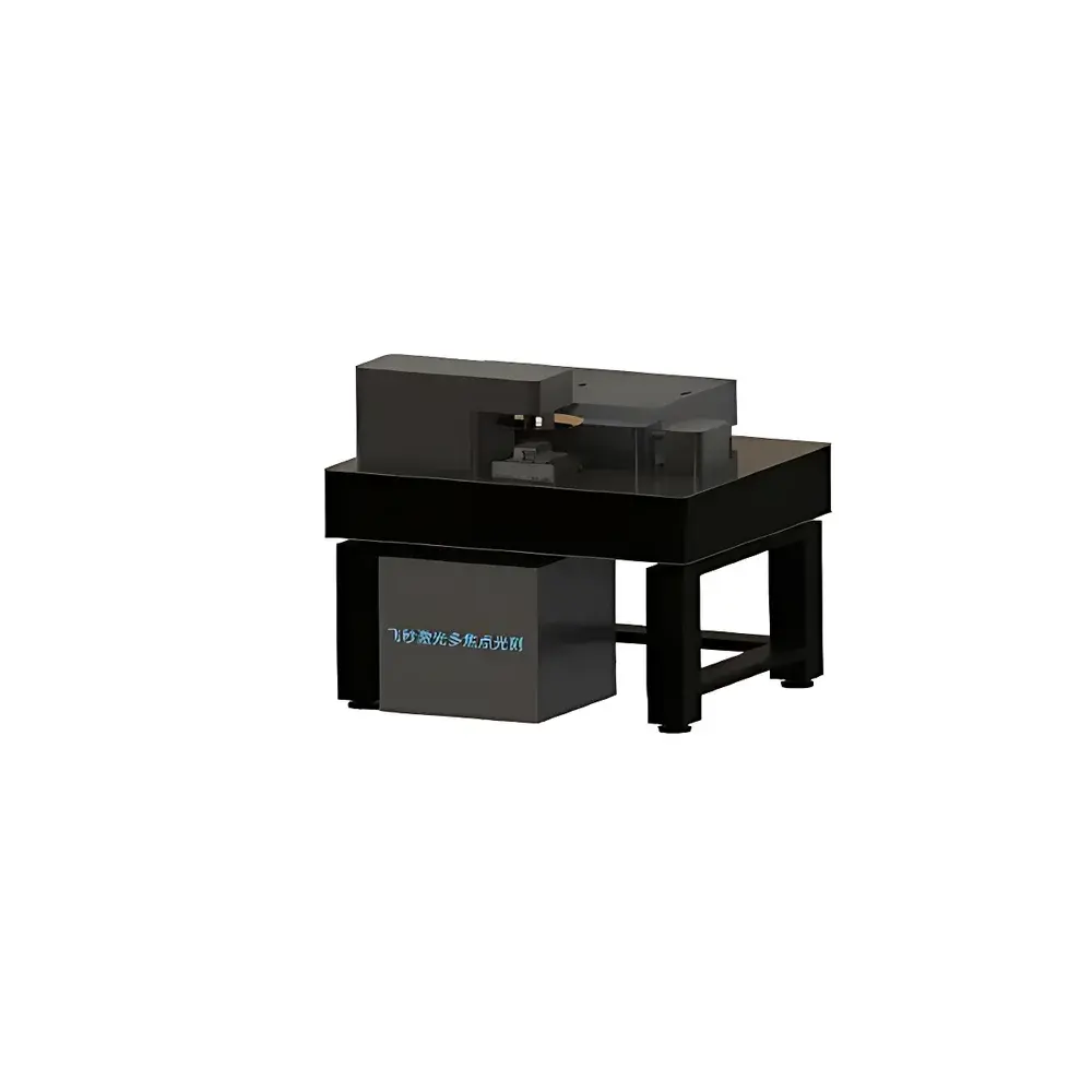
| Brand | Other brands |
|---|---|
| Origin | Hong Kong |
| Manufacturer Type | General distributor |
| Domestic/Imported | Domestic |
| Model | FP NanoPrinter |
| Price Range | USD 140,000 – 700,000 |
| Key Features | DMD-based dynamic holographic patterning |
| Laser Safety Class | Class 4 |
| XY/Z Feature Size | 142 nm / 175 nm |
| Resolution (Diffraction-Limited) | 285 nm / 500 nm |
| Layer Spacing | ≥ 0.05 µm |
| Throughput | 100 mm³/hr |
| Parallel Foci | ≥ 100 |
| Surface Roughness | ≤ 20 nm |
| Operating Temp | 23 ± 1 ℃ |
| RH | < 50% (recommended < 35%) |
| Vibration Requirement | Active isolation required |
| Power Supply | 220 V, > 35 A |
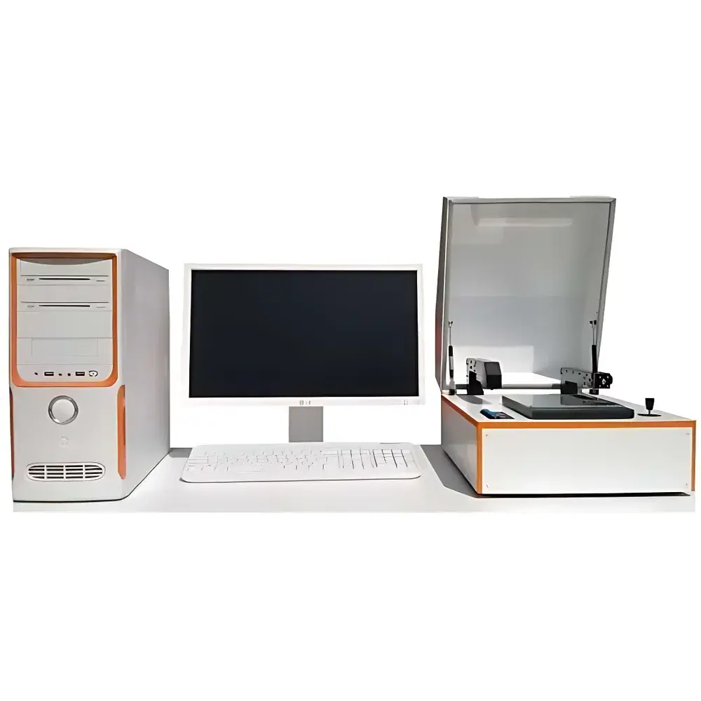
| Brand | pv-tools |
|---|---|
| Origin | Germany |
| Model | 4ppscan |
| Automation Level | Semi-Automatic |
| Max Test Current | 30 mA |
| Mapping Area | 10 × 10 cm |
| Measurement Duration (10×10 grid) | 4 min |
| Probe Tip Radius | 0.25 mm |
| Weight | 16 kg |
| Dimensions (L×W×H) | 36 × 48 × 24 cm |
| Vacuum Chuck Material | Borosilicate Glass |
| Probe Material | Tungsten Carbide |
| Software Features | Color-mapped resistivity visualization, histogram analysis, line-scan extraction, point re-measurement, I–V sweep linearity validation, auto-numbering |
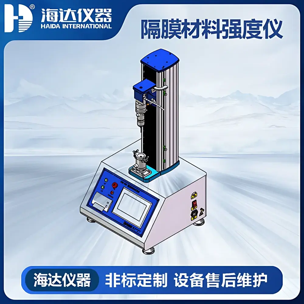
| Brand | HAIDA INTERNATIONAL |
|---|---|
| Origin | Guangdong, China |
| Manufacturer Type | Direct Manufacturer |
| Product Category | Domestic (PRC-Made) |
| Model | HAIDA HDV-001 Membrane Mechanical Strength Tester for Battery Separators |
| Pricing | Upon Request |
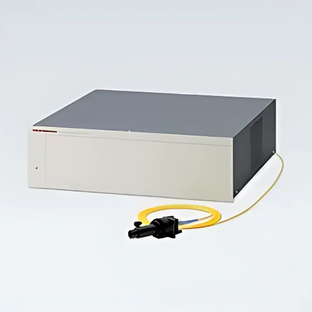
| Brand | Hamamatsu |
|---|---|
| Origin | Japan |
| Manufacturer Type | Original Equipment Manufacturer (OEM) |
| Product Category | Imported Instrumentation |
| Model | C11011 Series |
| Pricing | Available Upon Request |
| Measurement Principle | Laser Interferometry (Infrared, 1300 nm) |
| Max. Measurement Speed | 60 Hz |
| Spot Size | ≈ Ø60 µm |
| Working Distance | 155 mm (standard), optional 1000 mm |
| Thickness Range (Glass) | 25 µm – 2.9 mm |
| Thickness Range (Silicon) | 10 µm – 1.2 mm |
| Repeatability (Glass) | ±250 nm |
| Repeatability (Silicon) | ±100 nm |
| Accuracy (Silicon) | ±0.5 µm (≤500 µm), ±0.1% (>500 µm) |
| Max. Layers Measurable | 10 |
| Interface Options | RS-232C, Ethernet, USB 2.0, PIP (Hamamatsu Proprietary Interface Protocol) |
| Power Supply | AC 100–240 V, 50/60 Hz |
| Power Consumption | ~50 VA |
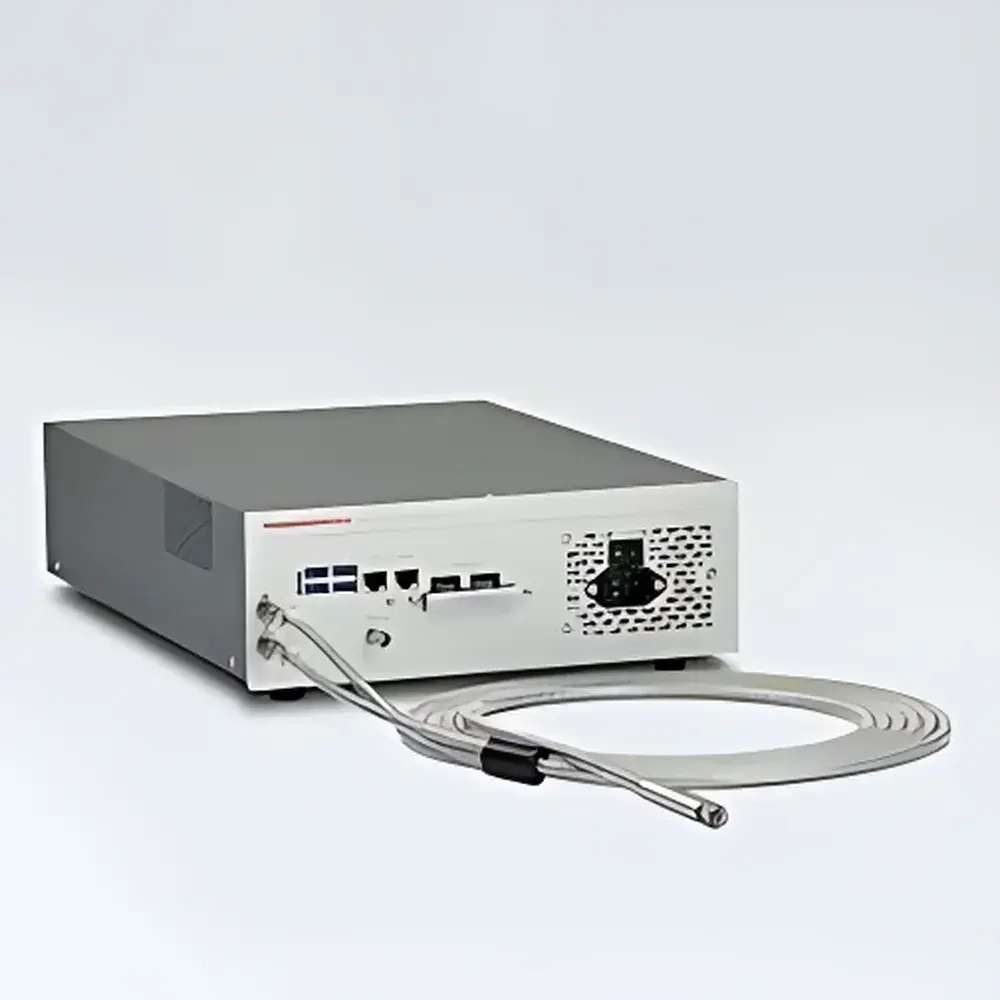
| Brand | Hamamatsu |
|---|---|
| Origin | Japan |
| Manufacturer | Hamamatsu Photonics K.K. |
| Type | Imported |
| Model | C12562-04 |
| Measurable Thickness Range (on glass substrate, n=1.5) | 500 nm – 300 µm |
| Measurement Repeatability (1 µm glass film) | ±0.2 nm |
| Measurement Accuracy | ±0.4% (per VLSI Standard Measurement Assurance Documentation) |
| Light Source | Halogen lamp |
| Spot Size | ~φ1 mm |
| Working Distance | 10 mm |
| Maximum Layers Analyzable | 10 |
| Analysis Modes | FFT, Curve Fitting, Optical Constant (n, k) Extraction |
| Measurement Speed | Up to 100 Hz (3 ms/point) |
| External Trigger Support | Enhanced TTL-compatible input |
| Interface | RS-232C, Ethernet |
| Power Supply | AC 100–240 V, 50/60 Hz |
| Power Consumption | ~80 VA |
| Fiber Connector | FC |
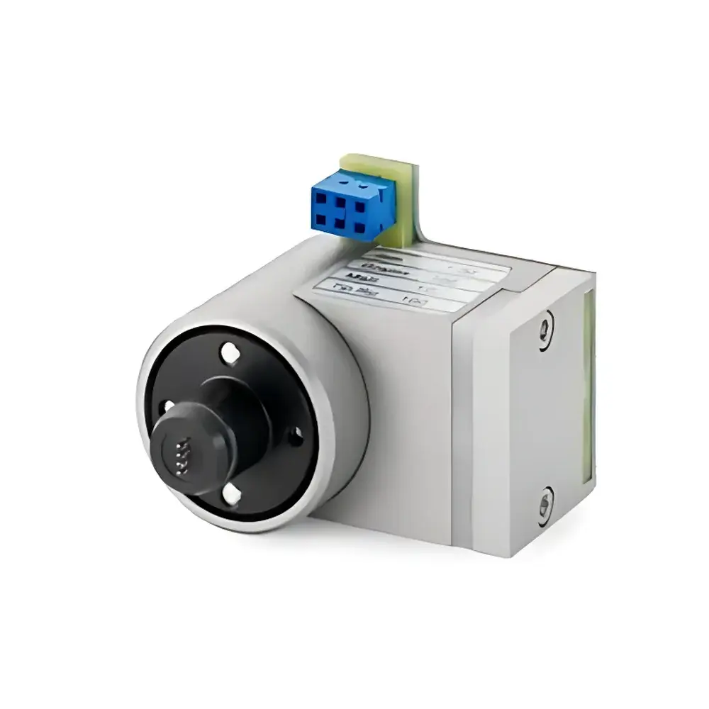
| Brand | Jandel |
|---|---|
| Origin | United Kingdom |
| Model | Cartridge |
| Probe Spacing Options | 0.500 mm, 0.635 mm, 1.00 mm, 1.27 mm, 1.591 mm (±10 µm tolerance) |
| Tip Material | Tungsten Carbide (standard) |
| Tip Diameter | 0.4 mm (standard), 0.3 mm (for high-density spacing) |
| Tip Radius of Curvature | 12.5, 25, 40, 100, 150, 200, 300, or 500 µm |
| Flatness | ≥ ±0.025 mm |
| Tip Load Range | 10 g to 250 g |
| Insulation Resistance | ≥10¹³ Ω at 500 V (between adjacent probes) |
| Probe Arrangement | Linear or rectangular |
| Buffer Zone | 0.5 mm |
| Automation Level | Manual |
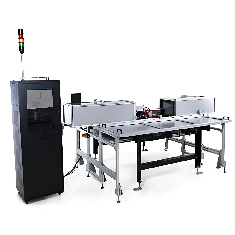
| Brand | k-Space Associates |
|---|---|
| Origin | USA |
| Manufacturer Status | Authorized Distributor |
| Origin Category | Imported |
| Model | kSA XRF |
| Price Range | USD $50,000 – $500,000 |
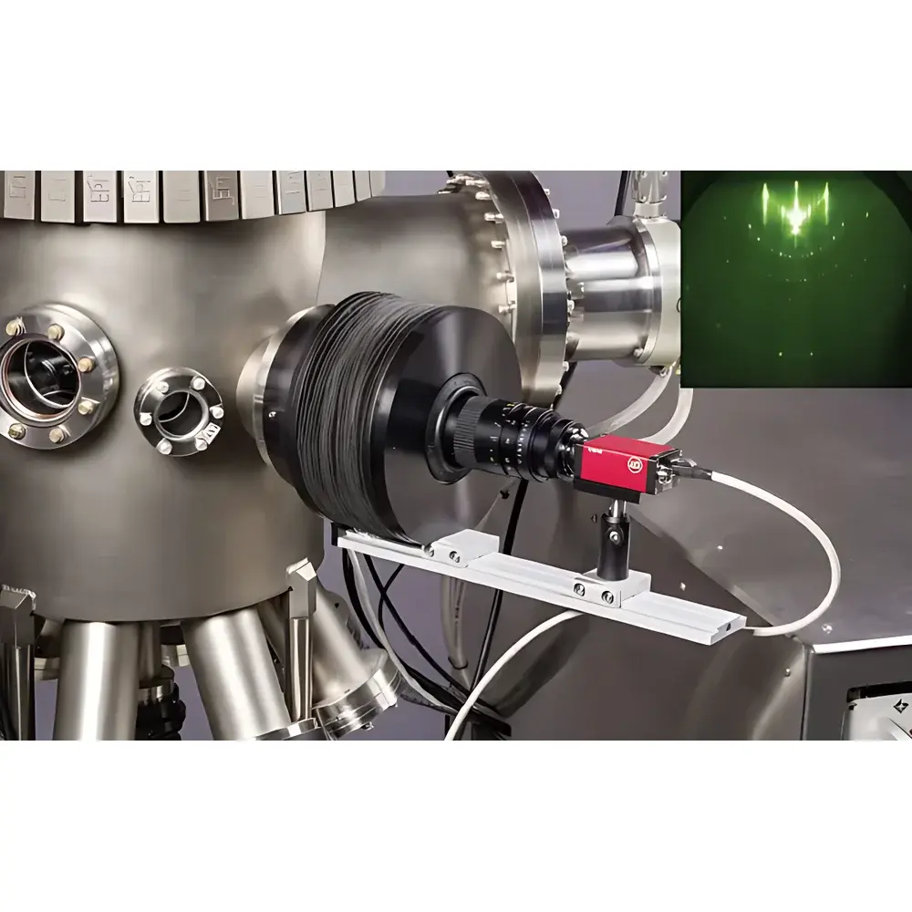
| Brand | k-Space |
|---|---|
| Origin | USA |
| Manufacturer Status | Authorized Distributor |
| Product Origin | Imported |
| Model | kSA 400 |
| Pricing | Upon Request |
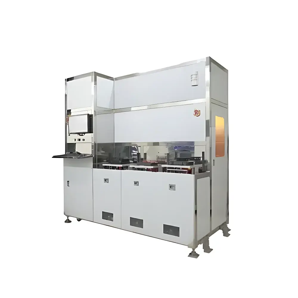
| Brand | Kainova |
|---|---|
| Origin | Taiwan |
| Manufacturer Type | Authorized Distributor |
| Product Category | Domestic (Taiwan-made) |
| Model | KAM-201 |
| Pricing | Upon Request |
| Reticle Handling Compatibility | EUV & Optical Reticles |
| Bonding Precision | ±0.1 mm |
| Post-Bonding Optical Distortion | <2 nm |
| Bonding Force Range | 0.035–0.4 kN |
| Cleanroom Particle Control | 0 EA for particles >100 nm |
| AMHS Integration | SEMI E84/E87 compliant |
| Vision-Based Alignment | Real-time image registration with dynamic parallelism compensation |
| AOI Inspection | Dedicated structured-light illumination for pellicle defect detection |
| Automated End-Effector Exchange | Yes |
| KAX-311 Reticle Transfer Module | Integrated rotational, flipping, and cassette exchange functions |
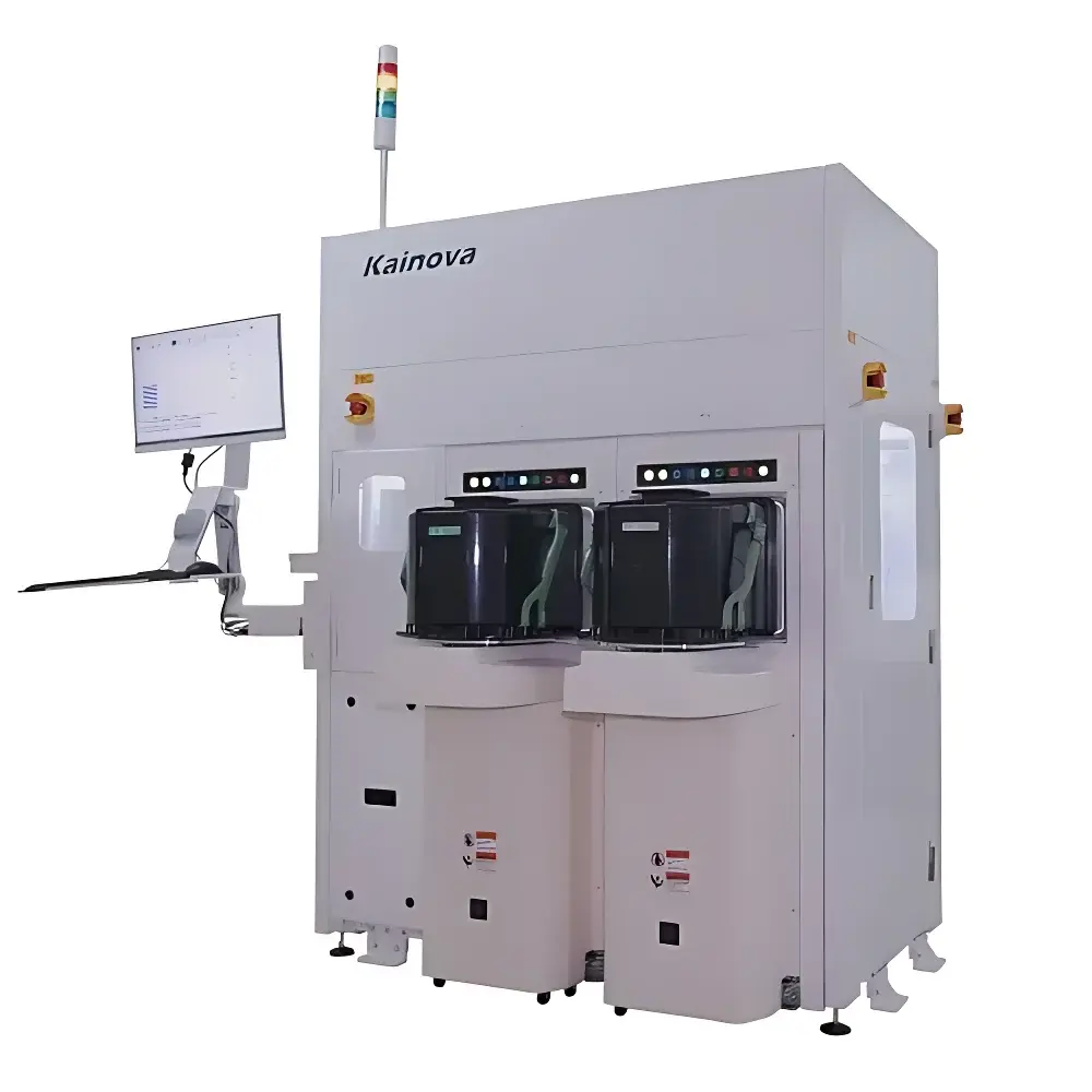
| Brand | Kainova |
|---|---|
| Origin | Taiwan |
| Manufacturer Type | Authorized Distributor |
| Product Category | Domestic (Taiwan-made) |
| Model | KAR-211 |
| Pricing | Upon Request |
| Load Ports | 2–8 configurable |
| Motion Control | 5-axis dual-end-effector robot |
| Wafer Compatibility | 200 mm (8″), 300 mm (12″), and thinned wafers (≤725 µm) |
| Dual-Side Wafer ID Reading | OCR + barcode (SEMI P17 compliant) |
| Interface Standards | SECS/GEM v2.0, SEMI E84 OHT Handshake Protocol |
| Cleanroom Certification | ISO Class 3 (FS-209E Class 1) |
| Throughput | ≥700 WPH |
| Positioning Accuracy | ±0.05 mm |
| Airflow Design | FFU-controlled laminar downflow with CFD-validated uniform velocity profile (0.45 ±0.05 m/s) |
| Safety & Compliance | SEMI S2-0215 Certified |
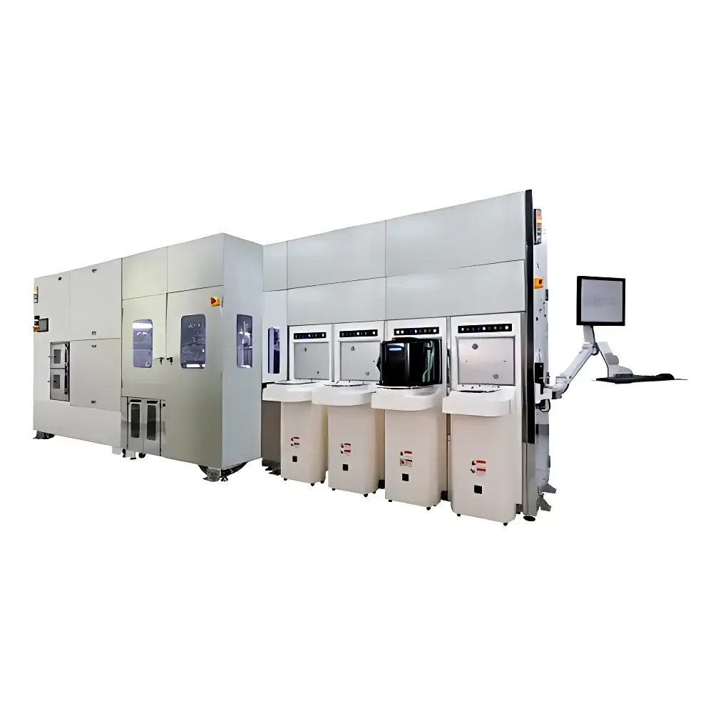
| Brand | Kainova |
|---|---|
| Origin | Taiwan |
| Manufacturer Type | Authorized Distributor |
| Product Origin | Taiwan |
| Model | Kainova Tech KAS-381 / KAS-382 / KAP-541 |
| Pricing | Upon Request |
| Maximum Cassette Capacity (KAS-381) | 87 FOUPs (2175 wafers) |
| Throughput | ≥180 WPH |
| Cleanroom Classification | ISO Class 4 (FS-209E Class 10) |
| Compatible Wafer Sizes | 200 mm and 300 mm |
| Substrate Compatibility | Standard and thinned wafers |
| Operating Environment | Nitrogen-purged (KAS-381/KAS-382) |
| Cassette Handling | Fully automated lid actuation, dual-lane unpacking/packing, recipe-driven sorting, batch merging/splitting, and Wafer ID–based routing |
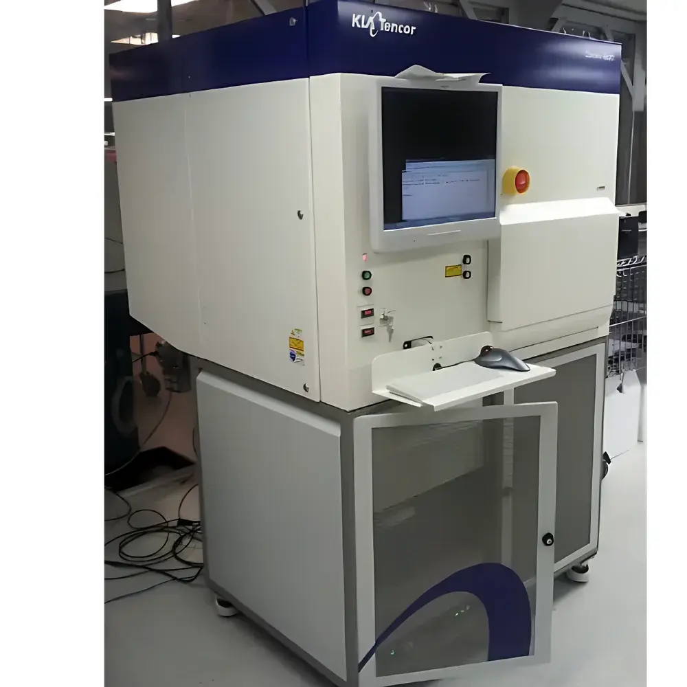
| Brand | KLA |
|---|---|
| Origin | Singapore |
| Manufacturer Type | Authorized Distributor |
| Origin Category | Imported |
| Model | Candela 8420 |
| Pricing | Available Upon Request |
| Instrument Category | Optical Non-Patterned Wafer Defect Inspection System |
| Primary Application | Surface Defect Detection on Unpatterned Wafers |
| Wafer Diameter | 2–8 inches |
| Throughput | 30 WPH |
| Resolution | 83 nm |
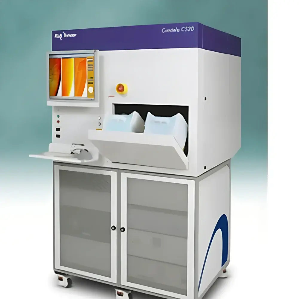
| Brand | KLA |
|---|---|
| Origin | Singapore |
| Manufacturer Type | Authorized Distributor |
| Origin Category | Imported |
| Model | CS20 |
| Quotation | Upon Request |
| Instrument Category | Optical Non-Patterned Wafer Defect Inspection System |
| Primary Application | Bare (Non-Patterned) Silicon Wafer Surface Defect Detection |
| Throughput | 30 WPH for 150 mm (6″) wafers, 27 WPH for 200 mm (8″) wafers |
| Resolution | 83 nm |
| Substrate Diameter Range | 50.8 mm – 200 mm (2″ – 8″) |
| Thickness Range | 350 µm – 1,100 µm |
| Minimum Detectable Defect Size | 0.3 µm (PSL sphere equivalent, ≥95% capture rate on bare Si) |
| Defect Types | Particles, scratches (≥100 µm × 0.1 µm × 50 Å), pits (≥20 µm Ø × 50 Å depth), stains (≥20 µm Ø × 10 Å thickness), bumps |
| Detection Threshold | Signal amplitude > 3× peak-to-valley background noise |
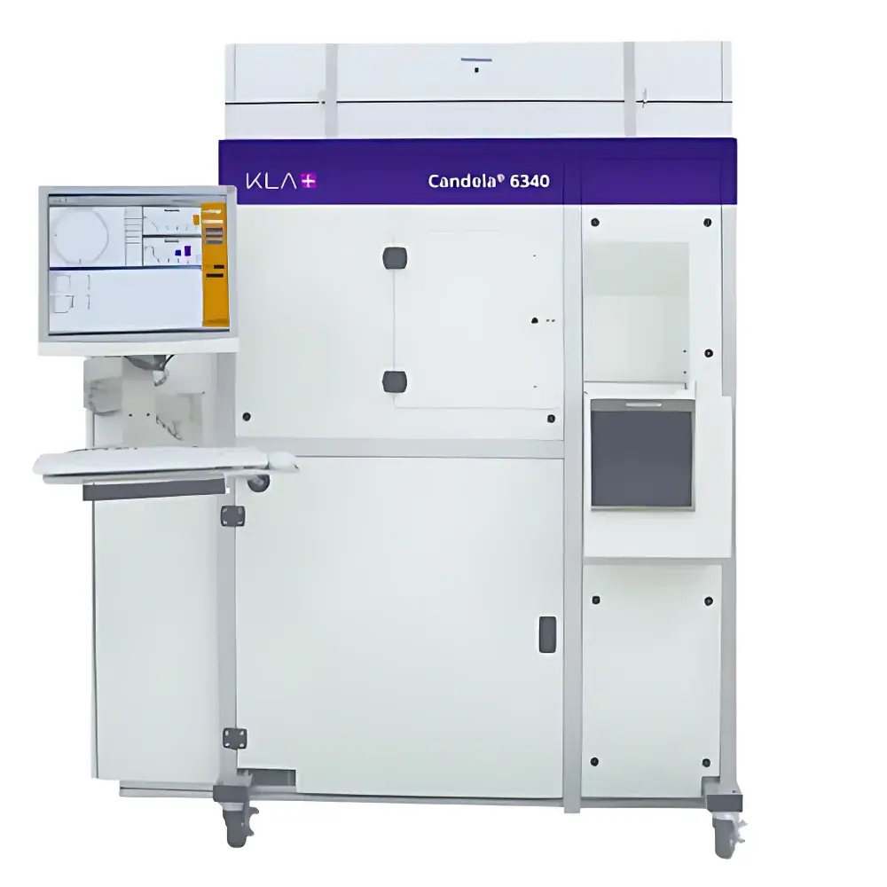
| Brand | KLA |
|---|---|
| Origin | USA |
| Manufacturer | KLA Corporation |
| Product Type | Optical Patterned Defect Inspection System |
| Model | Candela® 6300 |
| Detection Sensitivity | Sub-0.1 Å surface roughness change |
| Spatial Bandwidth | 0.22–2000 µm |
| Measurement Modes | Radial & tangential topography profiling, roll-off analysis, texture uniformity, particle/scratch detection |
| Compliance | Designed for semiconductor and data storage manufacturing environments |
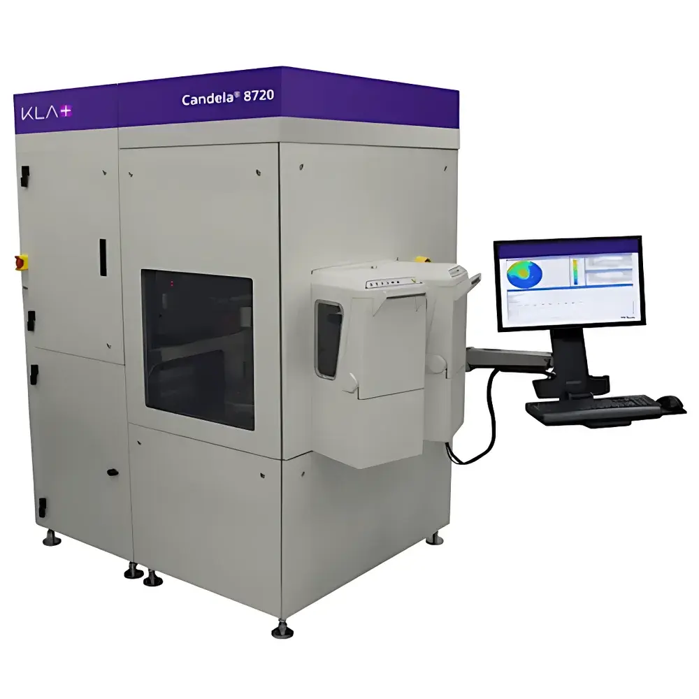
| Brand | KLA-Filmetrics |
|---|---|
| Origin | USA |
| Manufacturer Type | Authorized Distributor |
| Product Category | Imported |
| Model | Candela® 8720 |
| Instrument Type | Optical Patterned Wafer Defect Inspection System |
| Primary Application | Automated wafer inspection with Statistical Process Control (SPC) integration |
| Wafer Diameter | 200 mm |
| Detection Principle | Multi-angle elastic and inelastic scattering imaging |
| Key Capabilities | Simultaneous dual-angle scatterometry, surface topography mapping, reflectance profiling, phase contrast imaging, and photoluminescence (PL) detection |
| Compliance | Designed for semiconductor fab environments compliant with SEMI E30 (SECS/GEM), ISO 9001, and industry-aligned GLP/GMP data integrity expectations |
| Brand | KLA |
|---|---|
| Origin | Fujian, China |
| Manufacturer Type | Authorized Distributor |
| Country of Origin | China |
| Model | R50 |
| Price Range | USD $42,000 – $140,000 (FOB) |
| Automation Level | Fully Automated |
| Sheet Resistance Range | 5 mΩ/□ to 5 MΩ/□ |
| Measurement Accuracy | ±1% |
| Repeatability | <0.2% |
| XY Stage Options | 100 mm × 100 mm or 200 mm × 200 mm |
| Maximum Sample Diameter | 200 mm |
| Measurement Modes | Contact Four-Point Probe (4PP) and Non-Contact Eddy Current (EC) |
| Mapping Configurations | Linear, Rectangular, Polar, and User-Defined Grids |
| Compliance | ASTM F84, ISO 10474, SEMI MF67, USP <1031>, GLP/GMP-ready audit trail support |
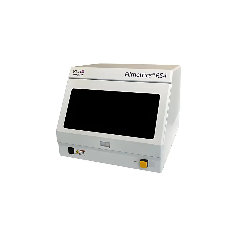
| Brand | KLA |
|---|---|
| Origin | USA |
| Model | R54 |
| Automation Level | Semi-Automatic |
| Resistivity Measurement Range | 1 mΩ/□ to 200 Ω/□ |
| Resistivity Measurement Accuracy | < 0.02% |
| Z-Travel Range | 15 mm |
| XY Stage Type | Motorized |
| Max Sample Height | 15 mm |
| Max Sample Weight | 2.5 kg |
| 4PP Measurement Repeatability | < 0.02% |
| EC Measurement Repeatability | < 0.2% |
| Compatible Sample Sizes | Up to 300 mm Ø or A4 (210 × 297 mm) |
| Probe Configurations | Customizable rectangular, linear, polar, and user-defined mapping patterns |
| Dual-Mode Operation | Four-Point Probe (4PP) and Non-Contact Eddy Current (EC) |
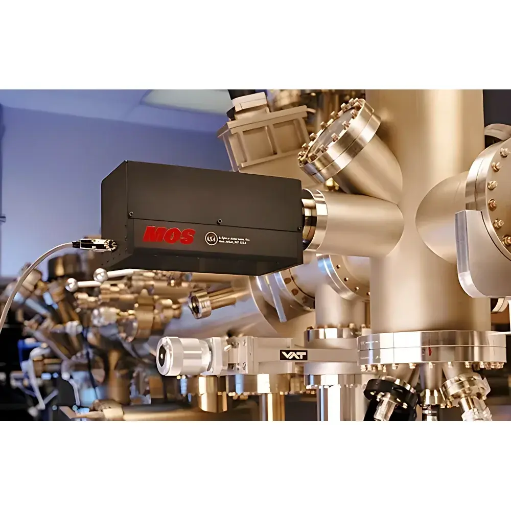
| Brand | k-Space Associates |
|---|---|
| Origin | USA |
| Model | kSA MOS |
| Stress Measurement Range | 0.32 MPa – 7.8 GPa |
| Measurement Technology | Multi-Beam Optical Sensor (MOS) |
| Operating Temperature | Ambient to system process temperature (vacuum chamber compatible) |
| Compliance | Designed for UHV/MBE/MOCVD integration, vacuum-rated optical interface, ISO 9001-manufactured instrumentation |
| Brand | k-Space Associates |
|---|---|
| Origin | USA |
| Manufacturer Status | Authorized Distributor |
| Origin Category | Imported |
| Model | kSA MOS TS |
| Price Range | USD 70,000 – 115,000 (approx.) |
| Stress Measurement Range | MPa to GPa |
| Measurement Technology | Multi-Beam Optical Sensor (MOS) Laser Array |
| Operating Temperature Range | RT to 1000°C |
| Curvature Resolution | ≥100 km radius detection limit |
| XY Scan Range | up to 300 mm (optional) |
| XY Scan Speed | up to 20 mm/s |
| XY Step Resolution | 2 µm |
| Compatible Wafer Diameters | 50 mm, 75 mm, 100 mm, 150 mm, 200 mm, 300 mm |
| Temperature Uniformity | ±2°C |
| Environmental Control | Vacuum & low-pressure inert/oxidizing gas (N₂, Ar, O₂) |
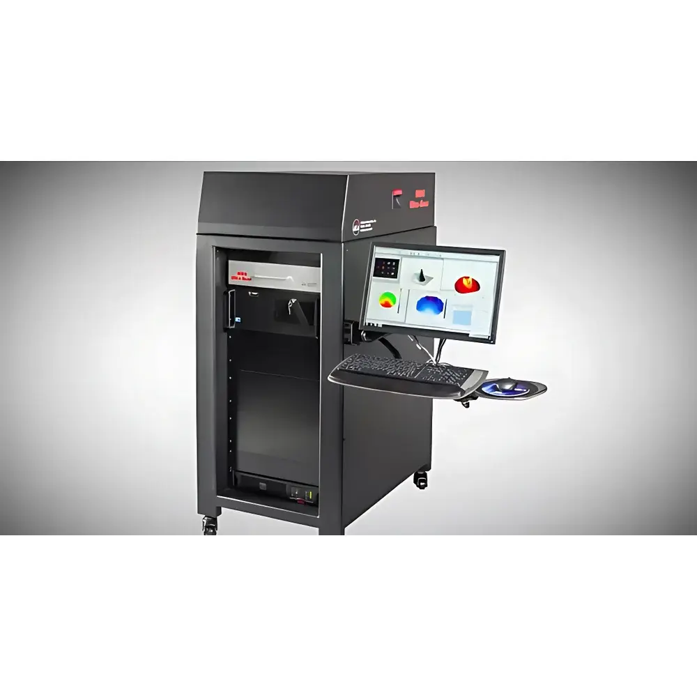
| Brand | k-Space |
|---|---|
| Origin | USA |
| Manufacturer Status | Authorized Distributor |
| Product Origin | Imported |
| Model | kSA MOS UltraScan |
| Stress Measurement Range | 0.32 MPa – 7.8 GPa |
| Measurement Technology | Multi-Beam Optical Sensor (MOS) Laser Array |
| Operating Temperature | Ambient or Variable-Temperature Mode |
| Brand | LEI-TECH |
|---|---|
| Origin | Tianjin, China |
| Manufacturer Type | Original Equipment Manufacturer (OEM) |
| Product Category | Domestic |
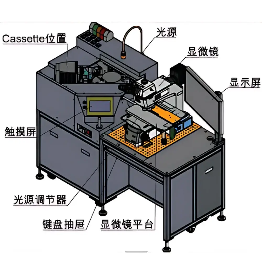
| Model | LK-BY86 |
| Pricing | Upon Request |
| Instrument Type | Optical Patterned Defect Inspection System |
| Primary Applications | Front-end & back-end wafer process monitoring, outgoing wafer quality control, automated wafer handling |
| Compatible Wafer Diameters | 150 mm (6″), 200 mm (8″), 300 mm (12″) |
| Brand | LEI-TECH |
|---|---|
| Origin | Tianjin, China |
| Manufacturer Type | OEM Manufacturer |
| Product Category | Domestic |
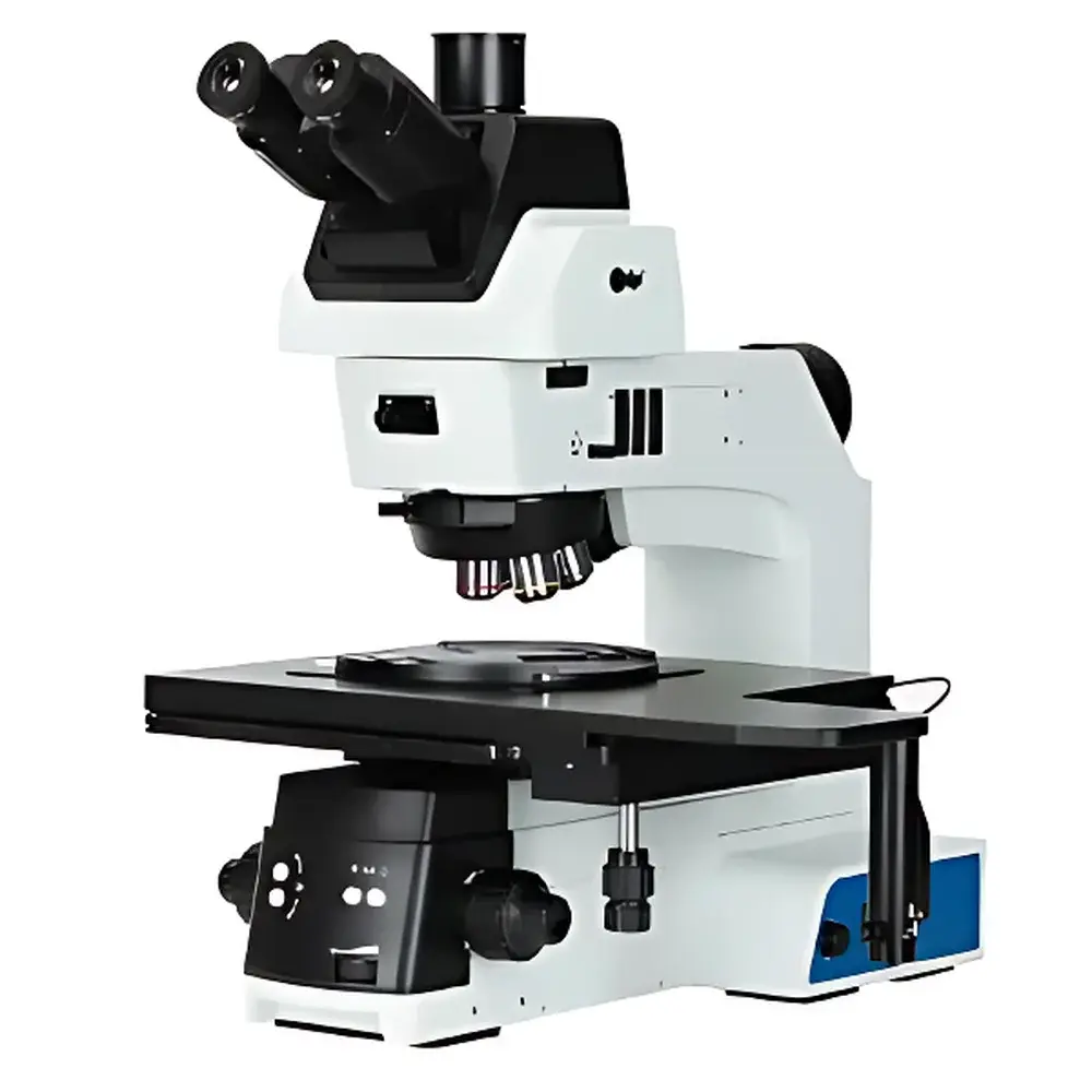
| Model | LK-ZDJY80R |
| Instrument Class | Optical Patterned Defect Inspection System |
| Primary Applications | Wafer process monitoring, outgoing wafer quality control |
| Compatible Wafer Sizes | 4", 6", 8", 12" |
| Brand | M&R |
|---|---|
| Origin | Taiwan |
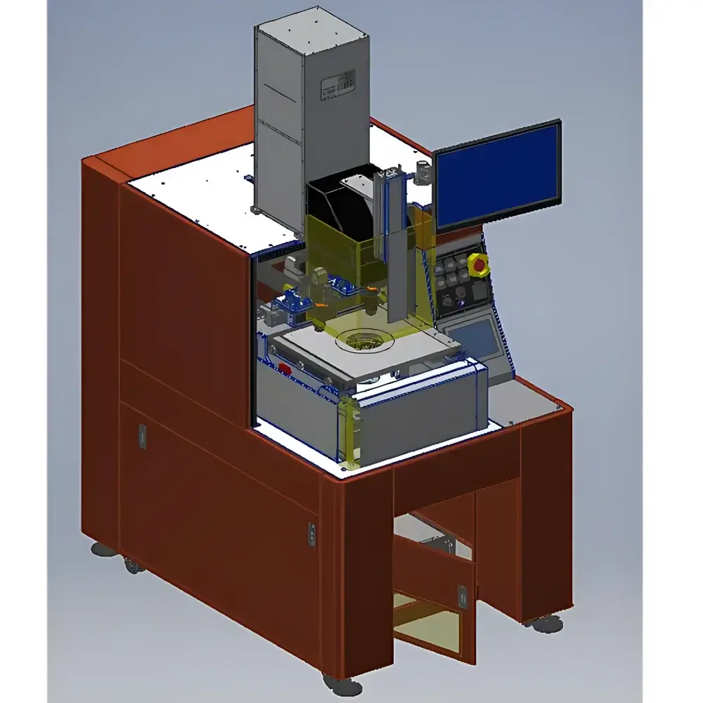
| Model | AA-8N-LED |
| Light Source | UV LED |
| Maximum Substrate Size | ≤4-inch wafers (including irregular shapes) |
| Overlay Alignment Accuracy | ±1 µm |
| Optical Resolution | ≤1 µm |
| Configuration | Standalone benchtop system for contact-mode lithography and manual/semi-automated bond alignment |
| Brand | Makeway |
|---|---|
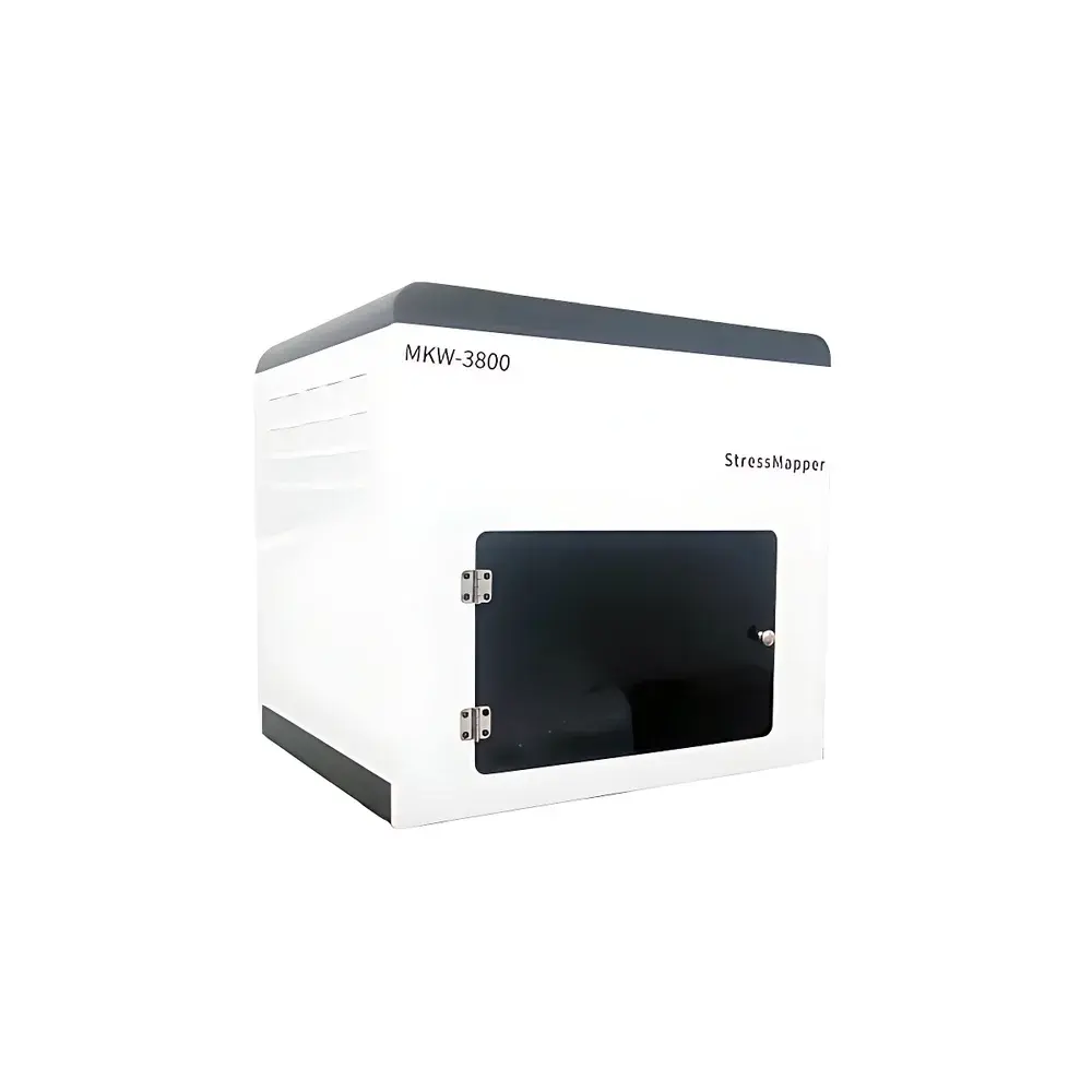
| Model | MKW-3800 |
| Origin | Shanghai, China |
| Measurement Principle | Non-contact structured light reflectometry |
| Sample Diameter | 2–8 inch wafers |
| Sampling Interval | down to 0.1 mm (full-field uniform sampling) |
| Measurement Time | <30 s (for 6-inch wafer, full aperture) |
| Warpage Range | 0.5–5000 µm |
| Warpage Repeatability | ±0.2 µm or ±1% |
| Warpage Accuracy | ±0.5 µm or ±1.5% |
| Stress Range | 1–10,000 MPa |
| Curvature Radius Range | 0.5–10,000 m |
| Curvature Repeatability | <1% (1σ @ 25 m radius) |
| Stress Repeatability | ±1.5 MPa or ±1% |
| Compatible Substrates | Si, GaAs, LiTaO₃, glass, sapphire, InP, SiC, GaN, bonded wafers, patterned wafers, square optical substrates |
| Compatible Films | Si, SiO₂, SiNₓ, Al₂O₃, TiO₂, photoresist, metal films, adhesives, nano-polymeric films, hybrid organic/inorganic films |
| Software | Stress Mapper (real-time acquisition, Stoney equation-based stress calculation, polynomial fitting, spatial filtering, ROI analysis, time-resolved & temperature-dependent stress profiling) |
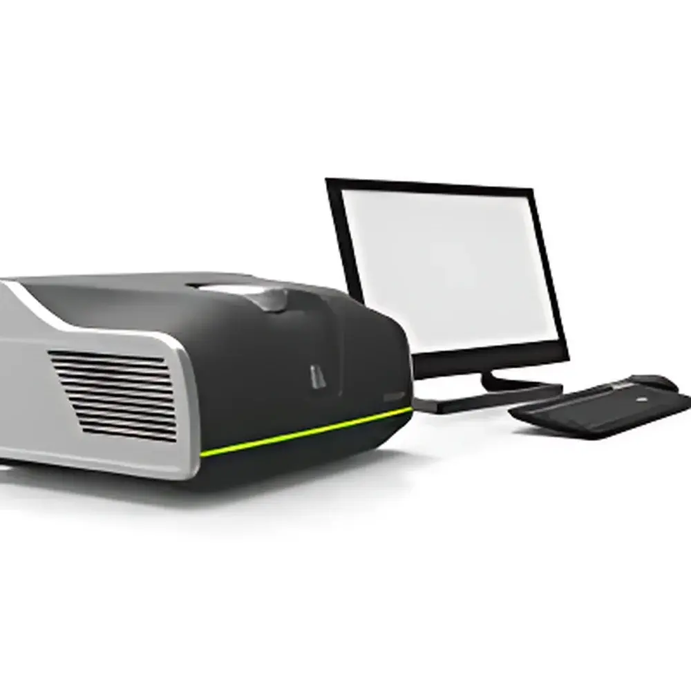
| Brand | Makeway |
|---|---|
| Model | MKW-2800 |
| Measurement Principle | 3ω Method |
| Temperature Control Range | Ambient to 200 °C (typical for thin-film thermal characterization) |
| Electrical Excitation Frequency | 1–10 Hz (optimized for 3ω harmonic detection) |
| Thermal Conductivity Range | 0.1–500 W/(m·K) |
| Resolution | <±2% (relative, under controlled lab conditions) |
| Compliance | ASTM E1461, ISO 22007-4, USP <1031> (thermal property validation) |
| Software Interface | Windows-based with real-time data acquisition, harmonic phase analysis, and temperature-swept conductivity mapping |
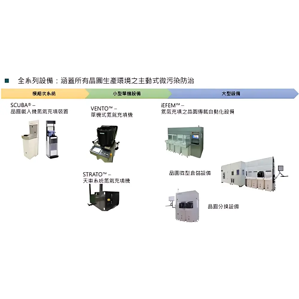
| Brand | KAINOVA |
|---|---|
| Origin | Taiwan |
| Manufacturer Type | Authorized Distributor |
| Regional Classification | Asia-Pacific Sourced |
| Model | Kainova Tech – Microcontamination Control Solution |
| Pricing | Available Upon Request |
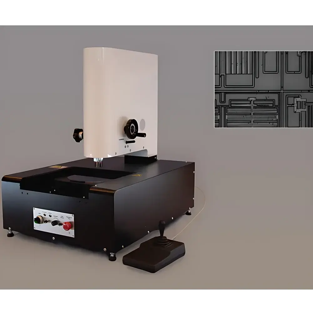
| Brand | Midas |
|---|---|
| Origin | Switzerland |
| Model | IR-M (Infrared Microscope) |
| Optical Magnification Options | 2.5×, 5×, 10× |
| Wafer Compatibility | 100 mm (4″), 150 mm (6″), 200 mm (8″) |
| Spatial Resolution | ≤3 µm (at 5× objective, transmission mode) |
| Detection Sensitivity | Defects ≥3 µm resolvable in Si wafers under IR transmission |
| Illumination Modes | Top-side visible illumination (reflected mode) + Through-wafer infrared illumination (transmission mode) |
| Imaging Sensor | IR-sensitive CMOS camera with USB 3.0 interface |
| Stage | Manual or motorized XY stage (Ø ≤200 mm wafer support) |
| Application Domain | Silicon IC & MEMS wafer-level defect inspection, SOI layer visualization, buried structure analysis |
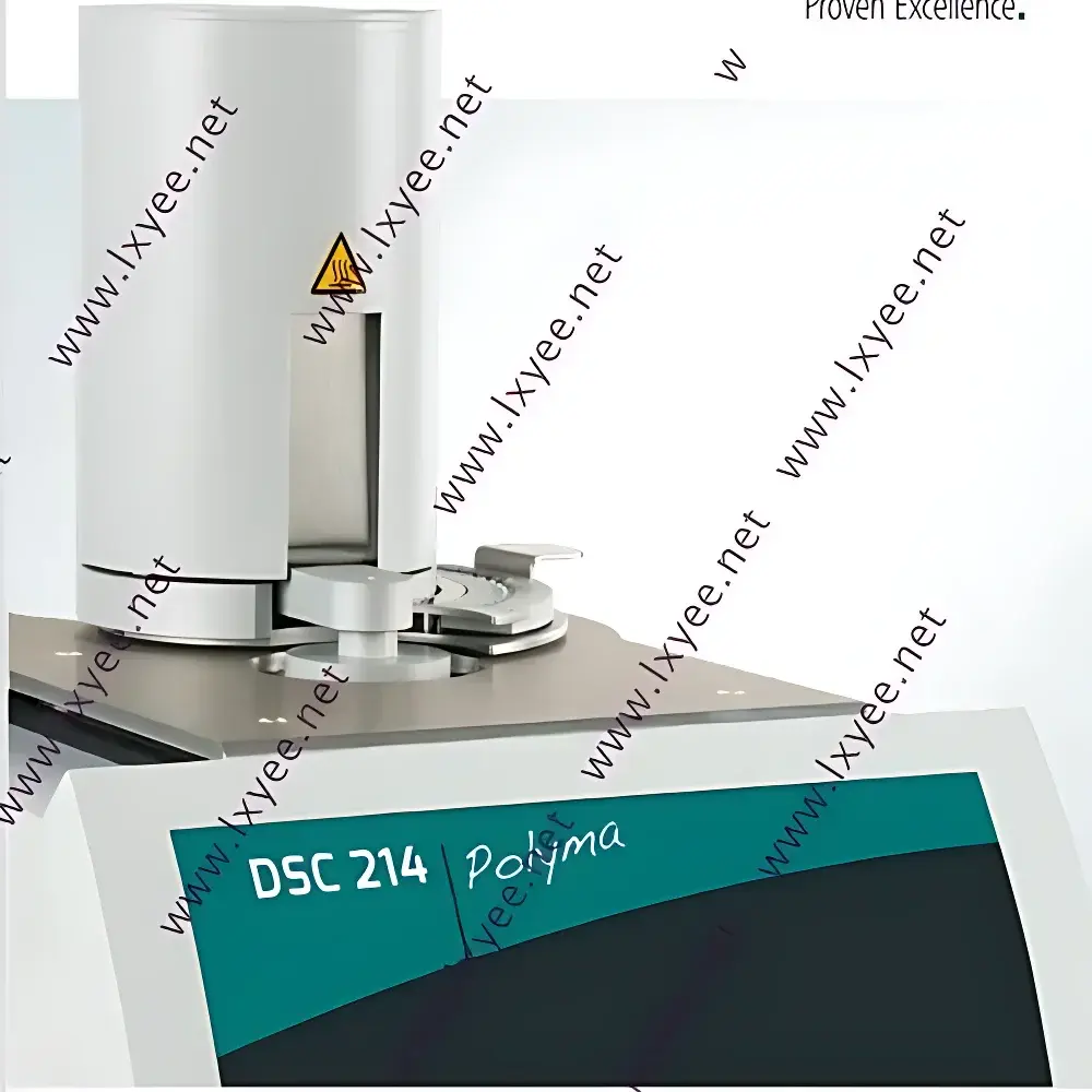
| Brand | Netzsch |
|---|---|
| Origin | Germany |
| Model | DSC 214 Polyma |
| Temperature Range | −100 °C to 600 °C |
| Heating/Cooling Rate | up to 500 °C/min |
| Sensor Type | Corona® high-reproducibility heat-flux sensor |
| Crucible System | Concavus® concave-bottom crucibles with fixed annular contact geometry |
| Software Platform | Proteus® with Smart Mode, Expert Mode, TM-DSC, Beflat® baseline correction, Auto-Analysis, Identify™ polymer recognition database |
| Compliance | ISO 11357-1, ASTM E794, ASTM E1356, USP <1151>, GLP/GMP-ready audit trail (FDA 21 CFR Part 11 optional) |
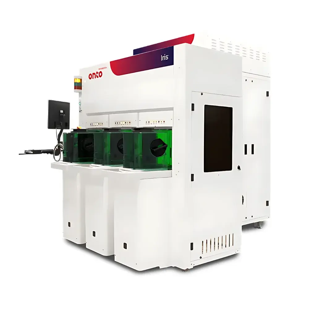
| Brand | AiYao Instruments |
|---|---|
| Origin | Malaysia |
| Manufacturer Type | Authorized Distributor |
| Origin Category | Imported |
| Model | IRIS S |
| Pricing | Available Upon Request |
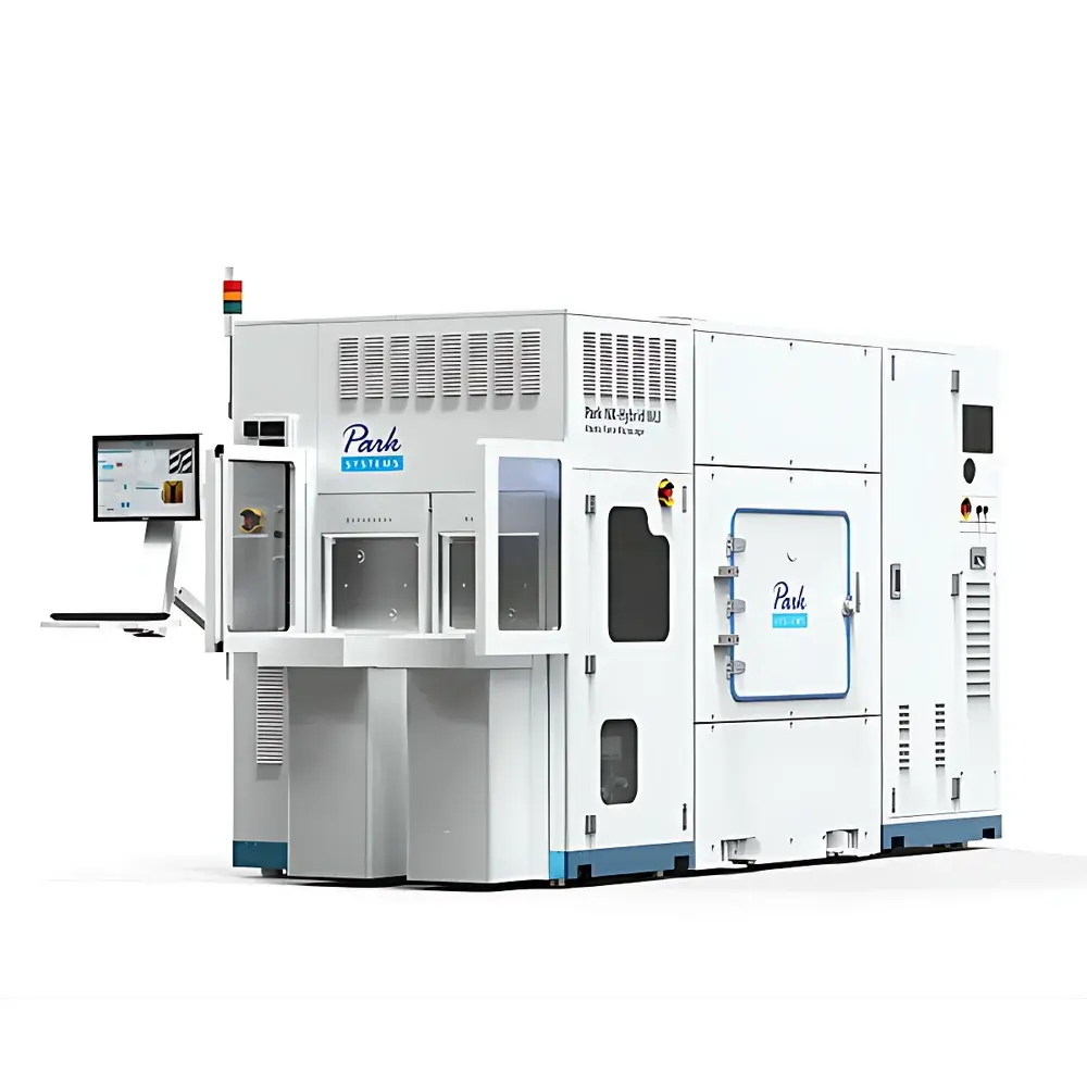
| Brand | Park SYSTEMS |
|---|---|
| Origin | South Korea |
| Model | NX-Hybrid WLI |
| Wafer Compatibility | 300 mm (fully backward-compatible with 200 mm and smaller wafers) |
| Instrument Category | Optical Defect Inspection & Hybrid Metrology System |
| Primary Application | In-line semiconductor process monitoring and defect characterization |
| Core Technology Integration | Co-registered AFM + WLI on single platform |
| Measurement Capability | Sub-ångström vertical resolution (AFM), nanometer-level lateral resolution, µm-to-mm field-of-view (WLI) |