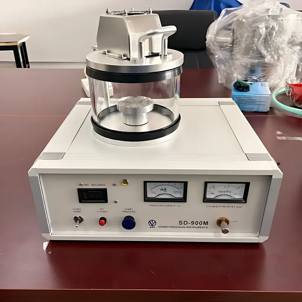
Boyuan Weina SD-900M Magnetron Sputter Coater
| Brand | Boyuan Weina / VPI |
|---|---|
| Origin | Beijing, China |
| Manufacturer Type | Authorized Distributor |
| Product Origin | Domestic (China) |
| Model | SD-900M Magnetron Sputter Coater |
| Target Materials | Au, Ag, Pt, etc. |
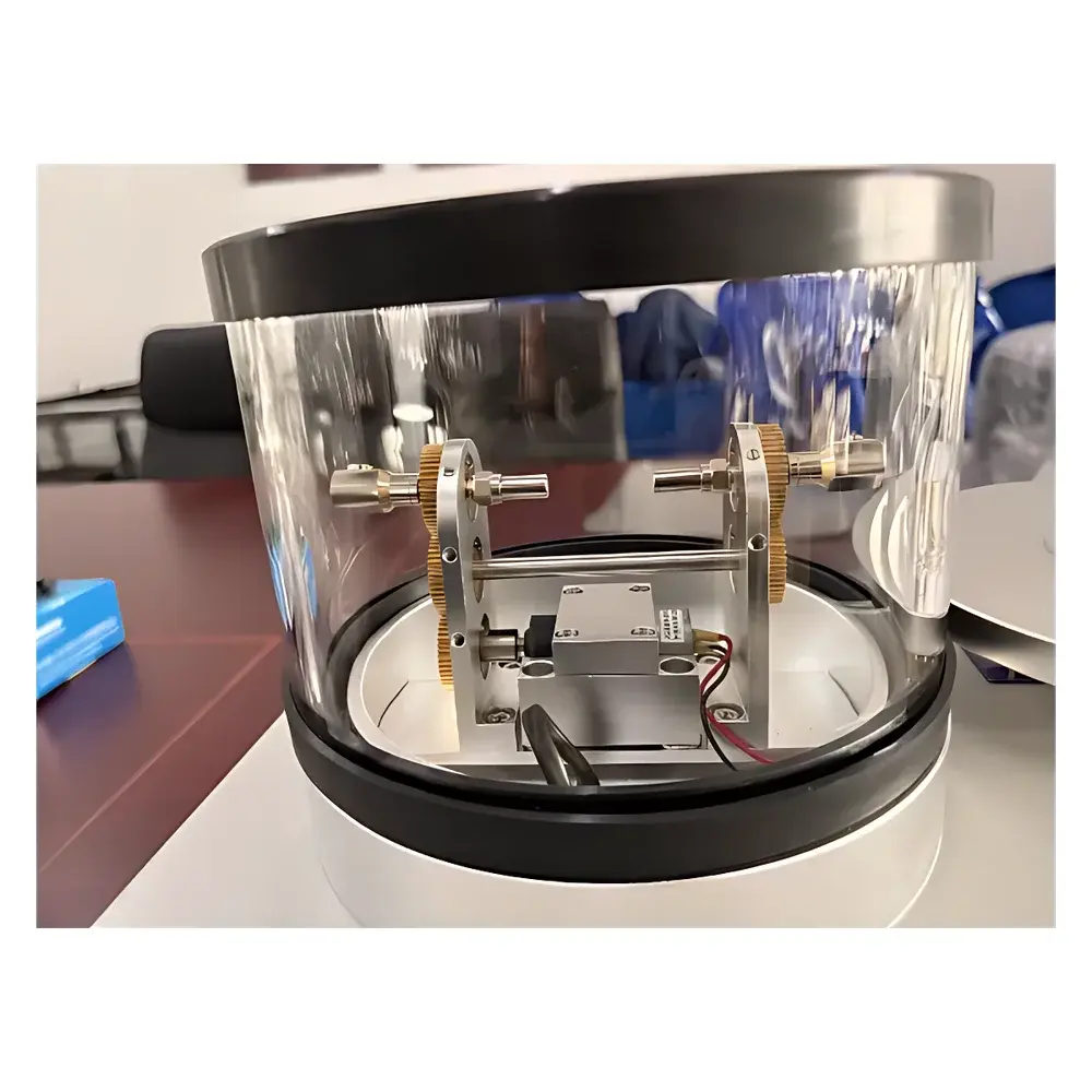
| Target Diameter & Thickness | φ50 mm × 0.1 mm |
| Control Mode | Manual and Programmable Auto Mode |
| Chamber Dimensions | φ160 mm × 120 mm (D × H) |
| Sample Stage Diameter | 50 mm (compatible with 70 mm optional) |
| Sputtering Gases | Ar, N₂, O₂, and other process gases |
| Maximum DC Voltage | −1600 V |
| Max Sputtering Current | 100 mA |
| Base Pressure | ≤4 × 10⁻² mbar |
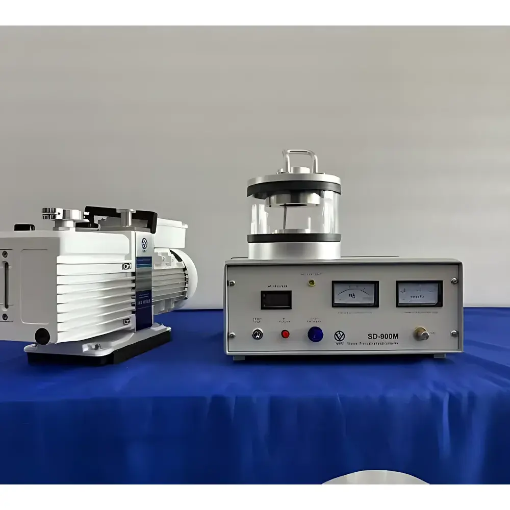
| Pumping Speed | 2 L/s (VRD-8 rotary vane pump) |
| Power Input | 220 V AC, 50 Hz (110 V option available) |
| Deposition Rate | ~40 nm/min (Au, under optimized Ar plasma conditions) |
Overview
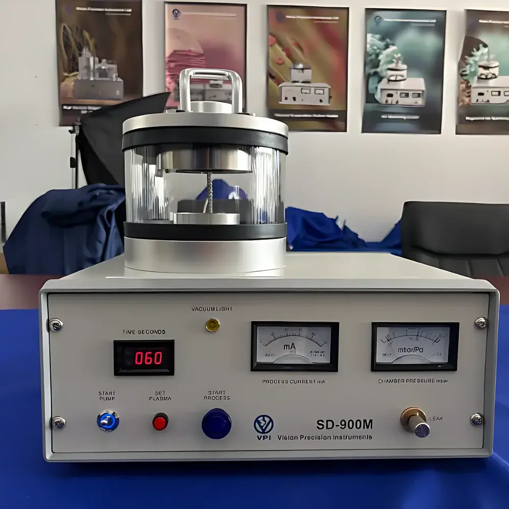
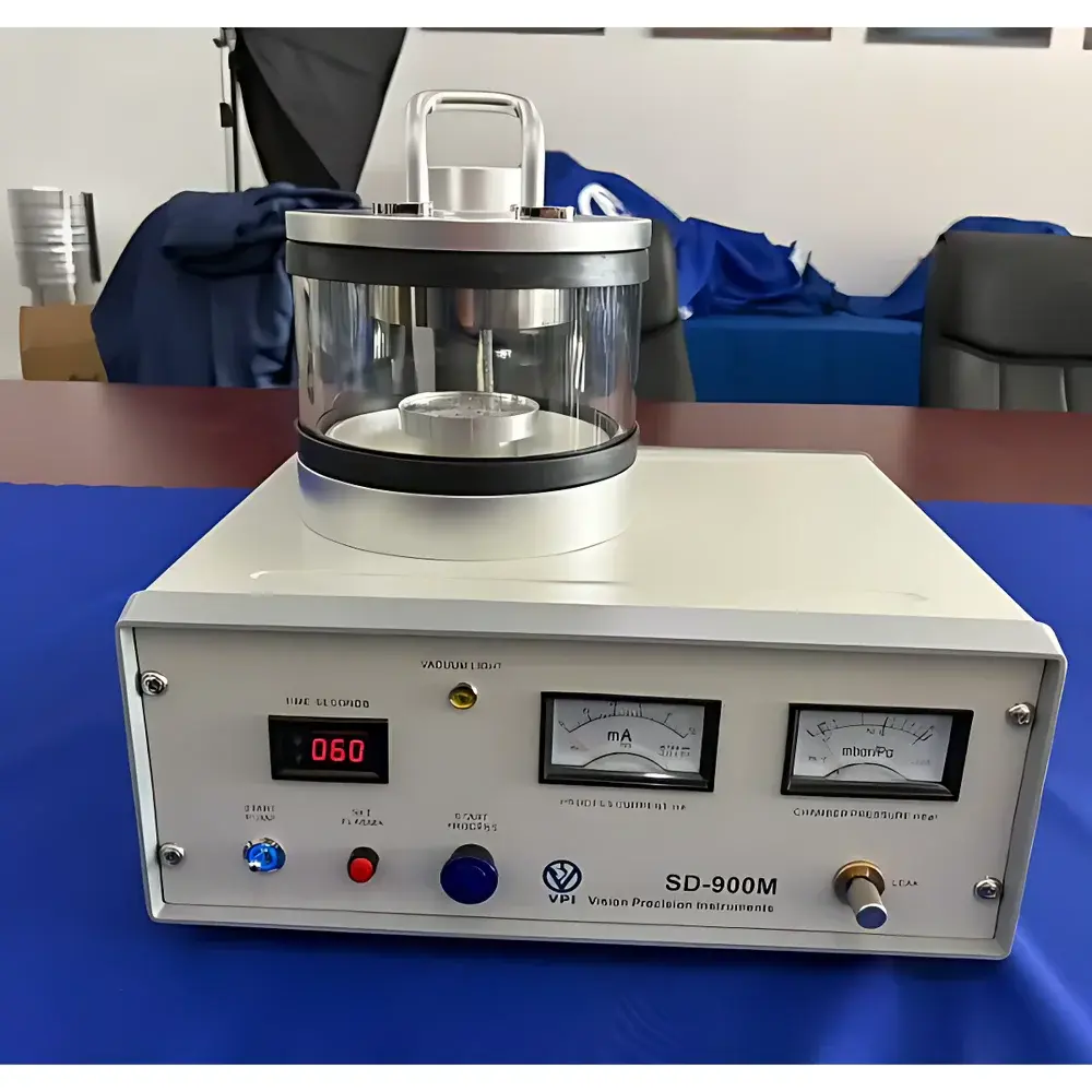
The Boyuan Weina SD-900M Magnetron Sputter Coater is a benchtop physical vapor deposition (PVD) system engineered for high-fidelity conductive coating of electron microscopy (EM) specimens. It employs magnetron-enhanced DC sputtering—a low-temperature, low-damage thin-film deposition technique—to produce uniform, nanoscale metallic layers on temperature-sensitive, non-conductive, or beam-sensitive samples. Unlike conventional diode sputtering, the SD-900M integrates permanent magnets behind the cathode target to confine electrons in closed-loop trajectories via Lorentz force interaction. This magnetic confinement increases ionization efficiency of the sputtering gas (typically argon), resulting in higher plasma density, enhanced sputter yield, and stable discharge at reduced operating pressures (≤4 × 10⁻² mbar) and lower substrate heating (<60 °C after 3 min operation). The system is optimized for applications demanding minimal thermal load, precise thickness control, and reproducible surface conductivity—particularly critical in scanning electron microscopy (SEM) sample preparation where charging, beam damage, and topographic fidelity must be rigorously managed.
Key Features
- Low-temperature operation: Maintains substrate temperature below 60 °C during standard 3-minute sputtering cycles—essential for preserving morphology of polymers, biological tissues, resins, and soft organic films.
- Dual-mode control: Supports both manual operation for rapid prototyping and programmable auto mode for repeatable, time-based deposition protocols (0–999 s digital timer).
- Modular target configuration: Standard 50 mm diameter × 0.1 mm thick gold target; compatible with optional Ag, Pt, Cr, Pd, and Ir targets for tailored secondary electron yield and X-ray transparency in EDS analysis.
- Optimized chamber geometry: Borosilicate glass vacuum chamber (φ160 mm × 120 mm) provides full visual access and accommodates up to 70 mm diameter sample stages (50 mm stage included).
- Integrated safety interlocks: Vacuum-pressure-dependent plasma cutoff prevents arcing at suboptimal pressure; over-current protection safeguards cathode and power supply.
- Gas flexibility: Equipped with micro-adjustable pneumatic valve for precise introduction of reactive gases (N₂, O₂) enabling nitride or oxide composite coatings.
- SETPLASMA pre-set function: Allows users to define threshold pressure and current values prior to ignition—minimizing transient overshoot and ensuring gentle plasma initiation for fragile specimens.
Sample Compatibility & Compliance
The SD-900M is routinely deployed for coating specimens incompatible with high-temperature or high-energy deposition methods. It meets routine laboratory requirements for SEM sample preparation per ASTM E1508-22 (“Standard Guide for Quantitative Analysis by Energy Dispersive Spectroscopy”) and supports GLP-compliant workflows when paired with audit-trail-capable external logging systems. Compatible sample types include:
- Beam-sensitive biological specimens (e.g., freeze-dried bacteria, pollen, insect cuticles)
- Non-conductive polymers and composites (e.g., PMMA, epoxy resins, hydrogels)
- Fragile thin films and 2D materials (e.g., graphene flakes, MOF crystals)
- Hygroscopic or volatile organics requiring cryo-compatible coating protocols
No internal heating elements or RF sources are present—eliminating risk of thermal degradation or dielectric breakdown. Chamber construction complies with IEC 61000-6-3 for electromagnetic emissions and features grounded stainless-steel shielding for stable DC discharge.
Software & Data Management
The SD-900M operates as a standalone hardware platform with analog/digital hybrid instrumentation: a calibrated vacuum gauge (Pirani-type), real-time ion current meter (0–100 mA), and digitally encoded timer. While it does not include embedded firmware or proprietary software, all operational parameters—including sputtering time, applied voltage, chamber pressure, and current—are directly observable and manually recordable. For laboratories requiring electronic data integrity under FDA 21 CFR Part 11 or ISO/IEC 17025, integration with external LabArchives, ELN systems, or custom Python-based acquisition scripts (via RS-232 or analog output ports) is fully supported. All calibration certificates for vacuum and current sensors are traceable to CNAS-accredited national standards.
Applications
- SEM sample preparation: Uniform Au or Pt coatings (2–10 nm) eliminate charging artifacts and enhance secondary electron emission for high-resolution imaging of insulators.
- TEM grid support film enhancement: Thin metal layers improve mechanical stability of carbon films during high-current beam exposure.
- Electrode fabrication for in-situ SEM testing: Localized sputtering enables direct metallization of microelectrodes on MEMS devices or battery cross-sections.
- Surface functionalization: Reactive sputtering with N₂ or O₂ yields TiN or ITO-like conductive layers for optoelectronic device prototyping.
- Reference material certification: Used in metrology labs to deposit certified-thickness reference films for AFM tip calibration and stylus profilometry validation.
FAQ
What vacuum level is required before initiating sputtering?
Base pressure must reach ≤4 × 10⁻² mbar using the integrated 2 L/s rotary vane pump. Final working pressure during sputtering is typically maintained between 5 × 10⁻² and 2 × 10⁻¹ mbar via adjustable gas inlet valve.
Can the SD-900M be integrated into a glovebox environment?
Yes—the system features a φ3 mm gas inlet port and flanged electrical feedthroughs, enabling seamless integration into inert-atmosphere gloveboxes for air-sensitive sample coating (e.g., perovskite precursors or lithium battery cathodes).
Is the sample stage cooled during operation?
No active cooling is provided; however, the low-power DC discharge and short duty cycles (<5 min) limit conductive and radiative heating. Measured surface temperature rise remains <15 °C above ambient for most substrates.
How often does the target need replacement?
Under typical SEM prep usage (2–5 nm Au layers, 30 s per sample), a standard 0.1 mm thick Au target lasts ≥200 coating cycles. Target erosion profile is monitored visually through the transparent chamber wall.
Does the system comply with CE or UL safety standards?
The SD-900M conforms to GB/T 18268.1-2010 (equivalent to IEC 61326-1) for electromagnetic compatibility and electrical safety in laboratory environments. CE marking is available upon request for EU-market configurations.


