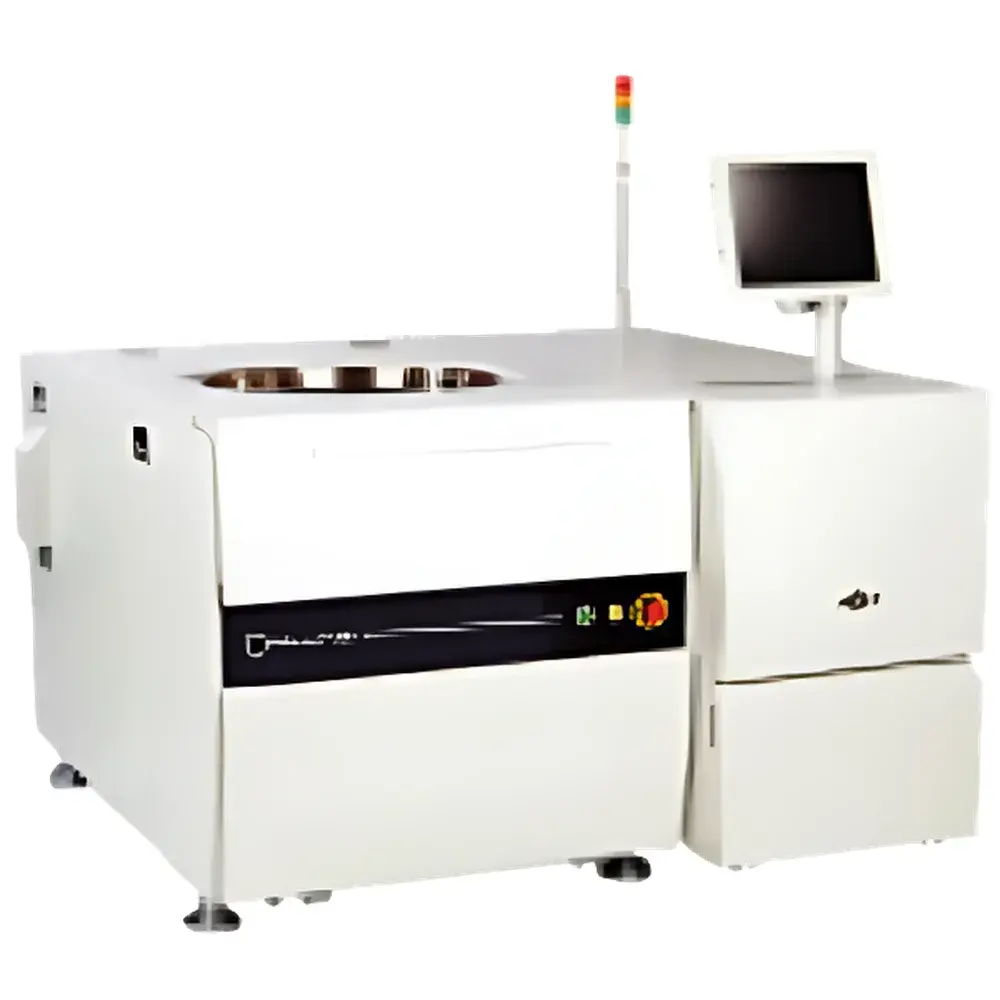
SEMICS OPUS Series Automated Wafer Probe Stations
| Brand | SEMICS |
|---|---|
| Origin | South Korea |
| Model | OPUS-SH / OPUS-SD / OPUS3 / OPUS-SS |
| Wafer Compatibility | 6", 8", and 12" (SEMI-compliant) |
| Dimensions (W×D×H) | OPUS-SH: 1490 × 1680 × 960 mm |
| OPUS-SD | 1530 × 1782 × 960 mm |
| XY Travel Range | ±175 mm (SH), ±185 mm × ±175 mm (SD) |
| XY Positioning Accuracy | ±1.5 µm |
| Maximum Downforce | 500 kgf |
| Temperature Range Options | Ambient to +150 °C, -40 °C to +150 °C, -55 °C to +200 °C, and 25 °C environmental chamber control |
| Structural Architecture | Rigid Z-frame with flat-load configuration |
| Key Functionalities | Real-time configuration validation, smart pin alignment algorithm, intelligent probing path optimization, map-shift prevention, drawer-type (SH) or universal probe card interface (SD/OPUS3), full pogo-pin tester compatibility |
Overview
The SEMICS OPUS Series represents a family of high-precision, fully automated wafer probe stations engineered for front-end semiconductor process development, device characterization, and production-level IC validation. Designed in strict adherence to SEMI standards (SEMI E10, E11, E30, E47), the platform supports 6-inch, 8-inch, and 12-inch silicon wafers—without mechanical reconfiguration—enabling seamless transition across technology nodes and product families. Each variant (OPUS-SH, OPUS-SD, OPUS3, and OPUS-SS) employs a rigid Z-frame architecture to minimize thermal drift and mechanical hysteresis, ensuring sub-micron repeatability in probe placement under dynamic load conditions. The system operates as an integrated electromechanical interface between automated test equipment (ATE) and bare-die wafers, delivering traceable, GLP-compliant electrical measurements through precisely controlled touchdown force (up to 500 kgf), real-time position feedback, and closed-loop thermal management.
Key Features
- Rigid Z-frame mechanical design optimized for long-term stability and minimal vibration coupling during high-speed probing cycles
- Flat-load wafer handling architecture reducing footprint by up to 22% compared to conventional tower-style stations
- Smart pin alignment algorithm leveraging real-time image correlation and sub-pixel centroid correction for <1.5 µm alignment accuracy
- Intelligent probing path optimization minimizing probe card wear and reducing average die-to-die move time by >35% versus fixed-grid navigation
- Map-shift prevention system utilizing dual-axis optical encoders and wafer edge recognition to correct for thermal expansion-induced coordinate drift
- Real-time configuration validation confirming probe card type, chuck temperature setpoint, force calibration status, and ATE handshake protocol prior to test initiation
- Modular thermal subsystem supporting multiple operational modes: ambient, heated-only (+25 °C to +150 °C), cryogenic (-55 °C to +200 °C), and precision environmental chamber control (±0.1 °C stability at 25 °C)
- Drawer-type probe card exchange mechanism (OPUS-SH) or universal probe card interface (OPUS-SD/OPUS3) enabling tool-change times under 90 seconds without recalibration
- Full compatibility with industry-standard pogo-pin-based testers—including Teradyne UltraFLEX, Advantest V93000, and Keysight PXI platforms—via IEEE-488, TCP/IP, and SECS/GEM protocols
Sample Compatibility & Compliance
The OPUS Series accommodates standard SEMI-compliant wafers (6”, 8”, and 12”) with notch/orientation flat detection per SEMI MF-1530. Chuck vacuum integrity is maintained across all diameters using segmented vacuum zones with independent pressure monitoring. Thermal uniformity across the platen meets SEMI E122 specifications (<±1.0 °C over 100 mm diameter at 125 °C). The system complies with IEC 61000-6-2 (immunity) and IEC 61000-6-4 (emission) for industrial environments, and supports FDA 21 CFR Part 11 audit trail requirements when integrated with validated MES or LIMS systems. Optional ISO Class 5 cleanroom-rated enclosures are available for high-reliability automotive and aerospace qualification testing.
Software & Data Management
The proprietary ProVision™ control software provides a unified GUI for hardware orchestration, recipe management, and real-time diagnostics. All motion parameters, thermal logs, force profiles, and alignment metrics are timestamped and stored in HDF5 format with SHA-256 checksums. Data export supports CSV, XML, and STDF v4.1 for direct integration into yield analysis platforms (e.g., PDF Solutions Yield Ramp, Synopsys Yield Explorer). Audit trails record operator ID, session start/end timestamps, parameter changes, and error events—fully compliant with GLP and GMP documentation requirements. Remote monitoring via TLS-secured WebSocket enables off-site engineering support with role-based access control (RBAC).
Applications
- Process development monitoring for advanced logic (FinFET, GAA), memory (DRAM, 3D NAND), and power devices (SiC, GaN)
- Parametric testing (Vt, Id-Vg, C-V, leakage) under temperature stress for reliability qualification (HTOL, ESD, TCT)
- Probe card validation and wear-life assessment using force-mapped touchdown profiling
- Automated failure analysis site localization via coordinated probe station–SEM–FIB workflows
- High-volume production screening for automotive-grade ICs requiring AEC-Q100 Grade 0/1 compliance
- Research applications including 2D material characterization and heterogeneous integration metrology
FAQ
Does the OPUS platform support both front-side and back-side probing?
Yes—optional back-side infrared illumination and through-wafer alignment modules are available for TSV and wafer-thinning applications.
What level of force repeatability is achieved across the full 500 kgf range?
Force control maintains ±0.5% full-scale repeatability over 10,000 cycles, verified per ASTM E4 and ISO 7500-1 calibration protocols.
Is remote software update capability supported?
Yes—over-the-air (OTA) firmware updates are delivered via encrypted SFTP with cryptographic signature verification and rollback protection.
Can the system be integrated into a Smart Factory environment?
Fully compatible with SEMI EDA/Interface A standards and supports MQTT 3.1.1 publishing for real-time equipment status telemetry to cloud-based MES platforms.
What documentation packages are provided for regulatory submissions?
Standard delivery includes IQ/OQ protocols, risk assessment (ISO 14971), traceable calibration certificates (NIST-traceable), and 21 CFR Part 11 validation templates for GxP environments.


