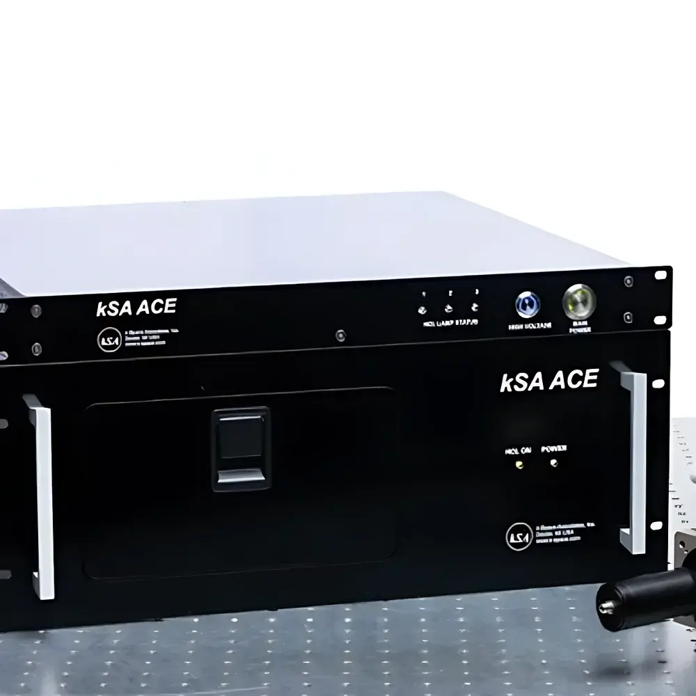
k-Space Associates kSA ACE In-situ Molecular Beam Flux Monitoring System
| Brand | k-Space Associates |
|---|---|
| Model | kSA ACE |
| Origin | USA |
| Vacuum Compatibility | Ultra-High Vacuum (UHV) / High Vacuum |
| Substrate Compatibility | Standard Semiconductor Wafers (e.g., Si, GaAs, InP, sapphire) |
| Source Flexibility | Unlimited (compatible with effusion cells, e-beam evaporators, magnetron sputter targets, PLD plumes) |
| Base Rotation | Supported |
| Optical Configuration | Triple Hollow Cathode Lamp (HCL) Integration |
| Detection Principle | Atomic Absorption Spectroscopy (AAS) |
| Element Capacity | Up to 3 elements simultaneously |
| Calibration Light Source | Pulsed Xenon Flash Lamp |
| Thermal Stability | Actively Temperature-Stabilized Optical Path |
| Data Interface | TCP/IP + Analog Voltage Output (0–10 V, proportional to absorbance/growth rate) |
| Software | kSA ACE Control & Analysis Suite (Windows-based, GLP-compliant logging) |
Overview
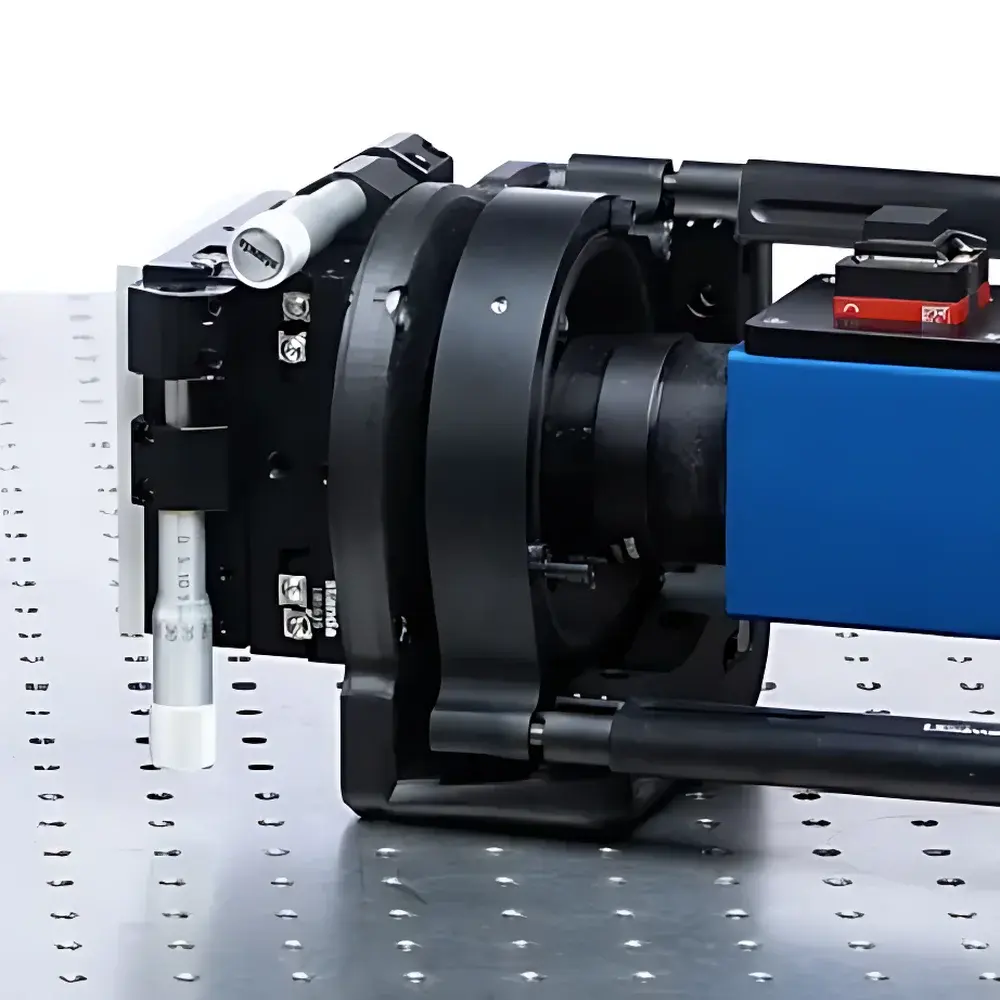
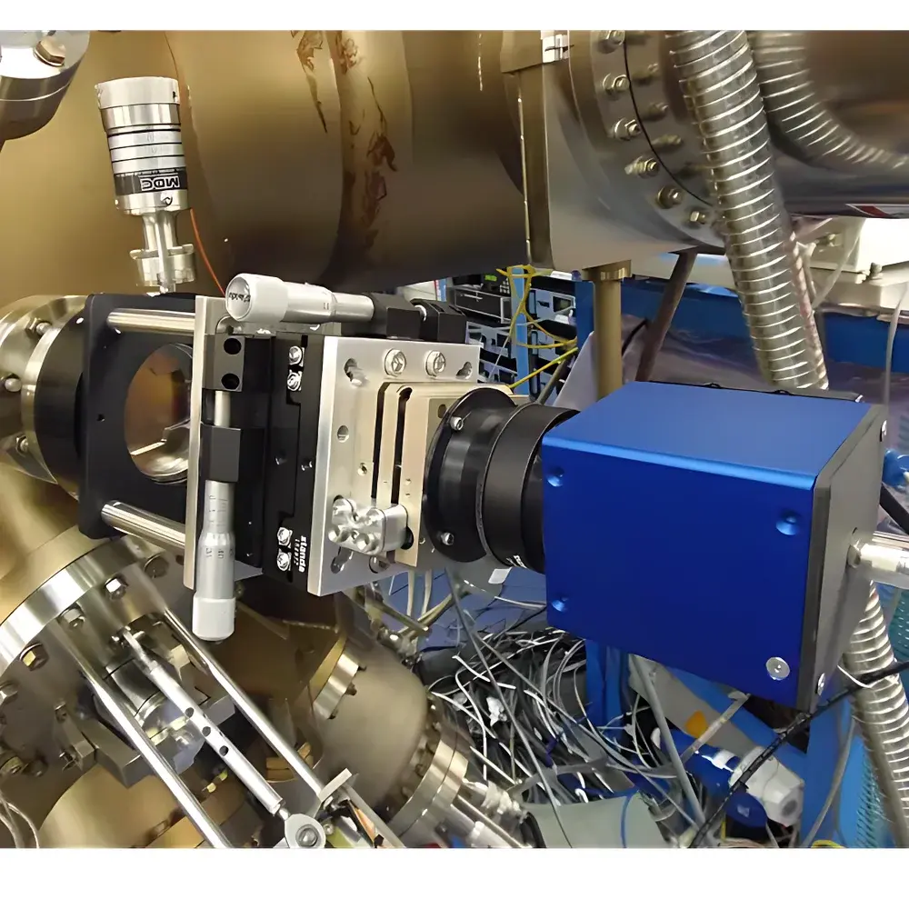
The k-Space Associates kSA ACE In-situ Molecular Beam Flux Monitoring System is a precision optical diagnostic instrument engineered for real-time, quantitative monitoring of atomic and molecular beam fluxes during thin-film growth under ultra-high vacuum (UHV) conditions. It operates on the fundamental principle of atomic absorption spectroscopy (AAS), where tunable narrow-linewidth emission from element-specific hollow cathode lamps (HCLs) is attenuated as it traverses the atomic vapor plume generated by evaporation or sputtering sources. The magnitude of spectral line attenuation—measured differentially between reference and signal channels—is directly proportional to the column density of the target species along the optical path, enabling absolute calibration of atomic flux (atoms·cm⁻²·s⁻¹) and instantaneous growth rate (Å/s). Designed for integration into MBE, PLD, thermal/e-beam evaporation, and magnetron sputtering systems, the kSA ACE delivers trace-level sensitivity (<1×10¹² atoms·cm⁻²·s⁻¹ detection limit for common III–V and II–VI species) without perturbing the deposition environment.
Key Features
- Triple-element capability: Simultaneous monitoring of up to three distinct atomic species via independently controlled HCLs, each emitting characteristic resonance lines (e.g., Ga 417.2 nm, As 402.9 nm, Al 396.2 nm)
- Dual-channel optical architecture: Reference channel continuously corrects for HCL intensity drift; signal channel quantifies absorption depth through the beam path, ensuring long-term measurement reproducibility (>99.5% stability over 24 h)
- Active thermal stabilization: Entire optical train—including fiber couplers, beam splitters, and spectrometer entrance optics—is housed in a temperature-controlled enclosure (±0.1 °C), minimizing thermal drift-induced wavelength shift and signal noise
- Viewport compensation: Integrated pulsed xenon flash lamp provides in situ correction for transmission loss caused by thin-film deposition on vacuum viewport windows, maintaining measurement fidelity across multi-day runs
- Real-time analog output: 0–10 V DC voltage signal proportional to absorbance (and thus flux or growth rate), compatible with standard PLCs, PID controllers, and feedback loops for closed-loop growth control
- Modular UHV-compatible design: All feedthroughs, lens mounts, and detector housings conform to CF-63/CF-100 flange standards; optical head integrates seamlessly with standard MBE chamber viewports (≥DN63)
Sample Compatibility & Compliance
The kSA ACE supports substrates ranging from 2″ to 8″ semiconductor wafers (Si, Ge, GaAs, InP, GaN-on-sapphire, MgO), including patterned and epitaxially masked configurations. Its non-invasive optical geometry imposes no constraints on substrate heating configuration—fully compatible with resistive, RF, or electron-beam heated stages operating up to 1100 °C. The system meets stringent UHV requirements (base pressure ≤1×10⁻¹⁰ Torr) and is routinely deployed in Class 100 cleanroom-integrated MBE facilities. All firmware and software logging functions comply with GLP (Good Laboratory Practice) and support 21 CFR Part 11 audit trails when configured with user authentication, electronic signatures, and immutable data archiving—essential for R&D validation and process transfer in compound semiconductor manufacturing.
Software & Data Management
The kSA ACE Control & Analysis Suite is a Windows-based application providing synchronized acquisition, real-time visualization, and post-run spectral deconvolution. It records time-stamped absorbance spectra at user-defined intervals (10 ms–10 s resolution), stores raw detector counts, calibrated flux values, and environmental metadata (chamber pressure, shutter status, source temperatures) in HDF5 format for interoperability with MATLAB, Python (h5py), and LabVIEW. The software includes built-in calibration wizards for HCL alignment, baseline correction, and multi-element spectral fitting using Voigt profile modeling. Export options include CSV, XML, and PDF reports compliant with ISO/IEC 17025 documentation standards. Remote operation via TCP/IP enables integration into factory-wide SECS/GEM or OPC UA automation frameworks.
Applications
The kSA ACE is deployed across academic, national lab, and industrial thin-film development platforms for stoichiometric control in compound semiconductor heterostructures (e.g., InGaAs/InP QW lasers, GaN HEMTs), photovoltaic absorber layers (CIGS, perovskite precursors), high-reflectivity dielectric stacks (TiO₂/SiO₂ for EUV optics), and X-ray multilayer mirrors (Mo/Si, W/B₄C). Its ability to resolve transient flux dynamics during shutter sequencing makes it indispensable for studying surface kinetics, adsorption/desorption barriers, and reactive co-evaporation processes. In production environments, it serves as a metrology backbone for SPC (Statistical Process Control) of layer thickness uniformity and composition drift across wafer batches.
FAQ
Does the kSA ACE require optical access through dedicated viewports?
Yes—it requires two aligned UHV-compatible viewports (one for incident beam entry, one for exit or reflection geometry), typically DN63 or larger, with anti-reflection coated fused silica or CaF₂ windows.
Can it monitor molecular species such as As₂ or Ga₂?
No—the system is optimized for atomic resonance lines; diatomic or cluster species require complementary techniques (e.g., quadrupole mass spectrometry or laser-induced fluorescence).
Is calibration traceable to NIST standards?
Yes—k-Space provides factory calibration certificates referencing NIST-traceable HCL spectral line centers and certified absorbance standards for primary flux calibration.
What maintenance is required during extended UHV operation?
Annual verification of HCL output intensity and spectrometer pixel-to-wavelength mapping is recommended; no consumables or routine alignment are needed due to rigid, kinematic optical mounting.
How does it handle interference from background gas species?
The narrow spectral bandwidth (<0.005 nm FWHM) and lock-in detection scheme suppress broadband plasma emission and stray light; spectral fitting algorithms isolate target lines even in presence of overlapping Ar or O₂ emission in sputtering environments.


