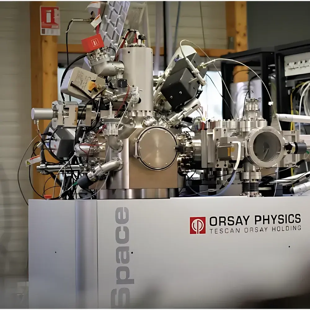
TESCAN Nanospace SIMS Orthogonal Time-of-Flight Secondary Ion Mass Spectrometry System
| Brand | TESCAN |
|---|---|
| Origin | Czech Republic |
| Manufacturer Type | Original Equipment Manufacturer (OEM) |
| Origin Category | Imported |
| Model | Nanospace SIMS |
| Instrument Type | Orthogonal Time-of-Flight (OTOF) SIMS |
| Mass Range | 1–1,500 Da |
| Mass Resolution | >9,500 (FWHM at m/z 100) |
Overview
The TESCAN Nanospace SIMS is an integrated ultra-high vacuum (UHV) focused ion beam scanning electron microscope (FIB-SEM) platform equipped with a high-performance orthogonal time-of-flight secondary ion mass spectrometry (OTOF-SIMS) analytical module. Engineered for nanoscale surface and near-surface chemical characterization, the system operates under base pressures below 1×10⁻¹⁰ mbar—ensuring minimal surface contamination and enabling quantitative, reproducible analysis of native surface chemistry. Unlike conventional SIMS instruments requiring separate vacuum chambers or sample transfer, Nanospace SIMS performs in situ ToF-SIMS analysis directly on FIB-prepared cross-sections, lamellae, or planar surfaces without breaking vacuum. Its core measurement principle relies on sputter-induced ionization: primary ion beams (e.g., O₂⁺, Cs⁺, Auₙ⁺ clusters) bombard the sample surface, ejecting secondary ions that are extracted orthogonally into a field-free flight tube and resolved by their time-of-flight—yielding high mass accuracy, isotopic fidelity, and sub-micrometer lateral resolution.
Key Features
- Integrated UHV FIB-SEM platform with <1×10⁻¹⁰ mbar base pressure, eliminating adsorbate interference and preserving true surface stoichiometry.
- ExOTOF™ secondary ion extraction column coupled with orthogonal acceleration ToF mass analyzer—delivering mass resolution >9,500 (FWHM at m/z 100) and mass range 1–1,500 Da.
- Nanometer-precise correlation between high-resolution SEM imaging, EDS elemental mapping, and EBSD crystallographic analysis—all performed in the same chamber without sample relocation.
- In situ ToF-SIMS analysis of FIB-milled cross-sections and TEM lamellae, enabling 3D molecular and isotopic tomography with depth resolution down to ~1 nm per slice.
- Multi-source FIB capability: interchangeable primary ion sources (O₂⁺, Cs⁺, Au₃⁺, Bi₃⁺, C₆₀⁺) optimized for enhanced ion yield, reduced fragmentation, and matrix-independent sensitivity.
- Cryogenic stage (down to –180 °C) for beam-sensitive organic, polymeric, and biological specimens—preserving molecular integrity during sputtering and ion detection.
- Automated multi-modal acquisition workflows: synchronized FIB milling, SEM navigation, and ToF-SIMS rastering controlled via unified software architecture.
Sample Compatibility & Compliance
The Nanospace SIMS accommodates conductive and insulating materials—including semiconductors, thin-film devices, geological specimens, pharmaceutical formulations, and cryo-preserved biological tissues—without mandatory conductive coating. Charge compensation is achieved via low-energy electron flood gun and adaptive biasing. All hardware and software modules comply with ISO/IEC 17025:2017 requirements for analytical laboratory competence. Data acquisition and processing support audit trails compliant with FDA 21 CFR Part 11 and EU Annex 11 for regulated environments. The system meets ASTM E1527-22 (Standard Guide for Use of SIMS in Surface Analysis) and ISO 18115-2:2017 (Surface Chemical Analysis — Vocabulary — Part 2: Terms Used in Secondary Ion Mass Spectrometry).
Software & Data Management
Acquisition and analysis are managed through TESCAN’s Unified Platform (UP) software suite, which provides fully traceable instrument control, real-time spectral visualization, and batch-processing pipelines for large hyperspectral datasets. Raw ToF-SIMS data are stored in vendor-neutral .imzML format, ensuring compatibility with open-source tools (e.g., SCiLS Lab, Hypermap, Python-based PyMCA). Multivariate statistical analysis—including PCA, MCR-ALS, and cluster analysis—is embedded for unsupervised identification of chemical species distributions. All processing steps—including peak integration, mass calibration, and depth profiling normalization—are logged with timestamped metadata, satisfying GLP/GMP documentation requirements.
Applications
- 3D dopant profiling in advanced logic and memory devices (e.g., FinFET, GAA transistors), resolving boron, phosphorus, and arsenic distributions at sub-5 nm depth intervals.
- Molecular layer characterization of OLED and perovskite photovoltaic stacks—mapping interfacial degradation products, ion migration pathways, and interdiffusion zones.
- Isotopic imaging of lithium-ion battery cathodes and solid electrolytes to quantify Li⁺ transport kinetics and SEI evolution across charge/discharge cycles.
- Subcellular metabolite mapping in frozen-hydrated tissue sections—enabling label-free spatial proteomics and lipidomics with cellular compartment resolution.
- Forensic analysis of trace contaminants on semiconductor wafers, including organic residues, metal oxides, and process-induced particulates.
FAQ
What vacuum level does the Nanospace SIMS achieve, and why is it critical for surface analysis?
The system maintains a base pressure below 1×10⁻¹⁰ mbar in the analysis chamber. This ultra-high vacuum minimizes hydrocarbon and water vapor adsorption—preventing artificial surface oxidation, carbon contamination, and signal suppression that compromise quantification accuracy.
Can the system perform depth profiling on insulating samples without charging artifacts?
Yes. Integrated low-energy electron flooding, variable sample bias, and pulsed extraction gating enable stable depth profiling on glasses, polymers, and oxides—with no need for metal coating or charge neutralization compromises.
How is data correlation handled between SEM, EDS, EBSD, and ToF-SIMS modalities?
All detectors share a common coordinate reference frame calibrated via stage metrology and fiducial markers. Spatial registration accuracy is ≤50 nm, allowing pixel-by-pixel overlay of compositional, crystallographic, and molecular maps within a single dataset.
Is the system compatible with regulatory-compliant laboratories?
Yes. Full 21 CFR Part 11 compliance—including electronic signatures, audit trails, user access controls, and data integrity validation—is implemented at the firmware and software layers.
What primary ion sources are available, and how do they affect molecular sensitivity?
Standard configurations include O₂⁺ (for electropositive elements), Cs⁺ (for electronegative species), and Au₃⁺/Bi₃⁺ clusters (for enhanced molecular ion yield and reduced fragmentation in organics). Optional C₆₀⁺ and Ar-GCIB sources are available for soft-landing analysis of fragile biomolecules.
Related Products
")