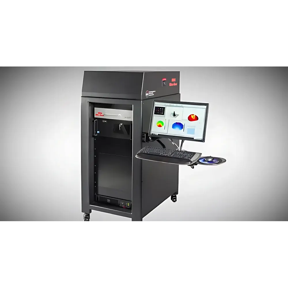
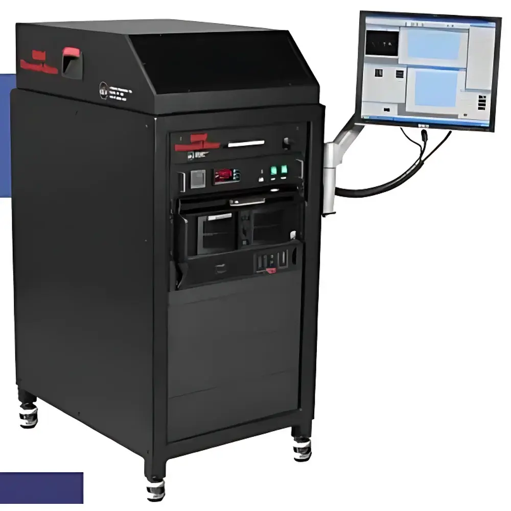
kSA MOS UltraScan Thin Film Stress Tester
| Brand | k-Space |
|---|---|
| Origin | USA |
| Manufacturer Status | Authorized Distributor |
| Product Origin | Imported |
| Model | kSA MOS UltraScan |
| Stress Measurement Range | 0.32 MPa – 7.8 GPa |
| Measurement Technology | Multi-Beam Optical Sensor (MOS) Laser Array |
| Operating Temperature | Ambient or Variable-Temperature Mode |
Overview
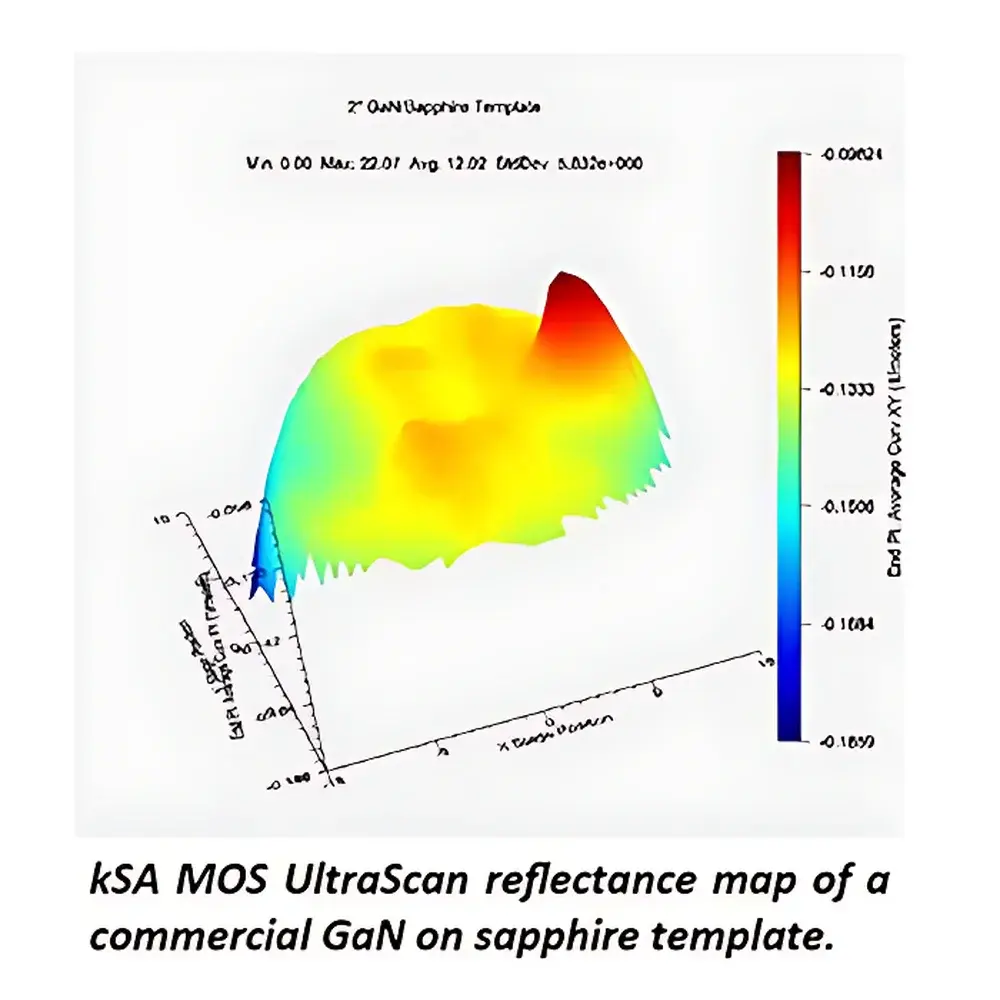
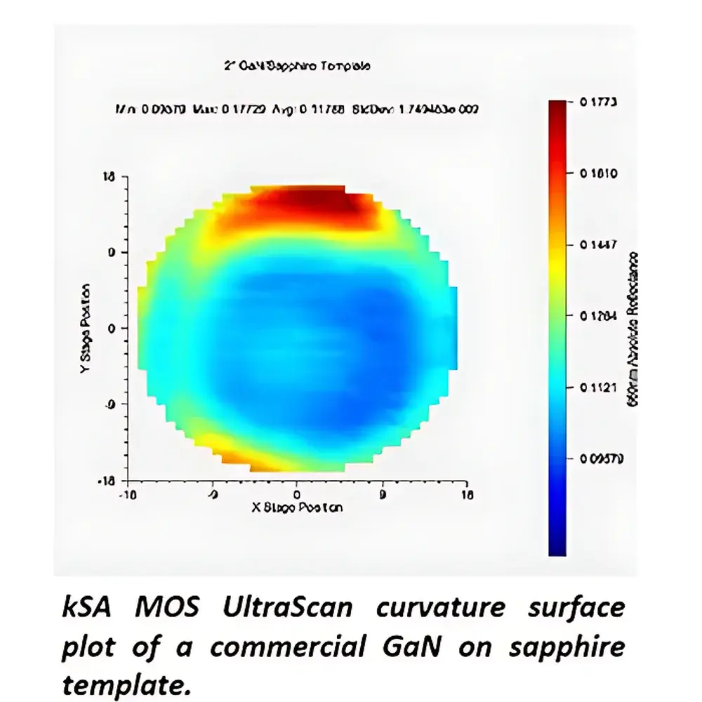
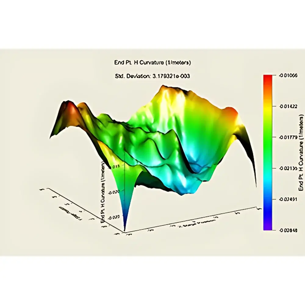
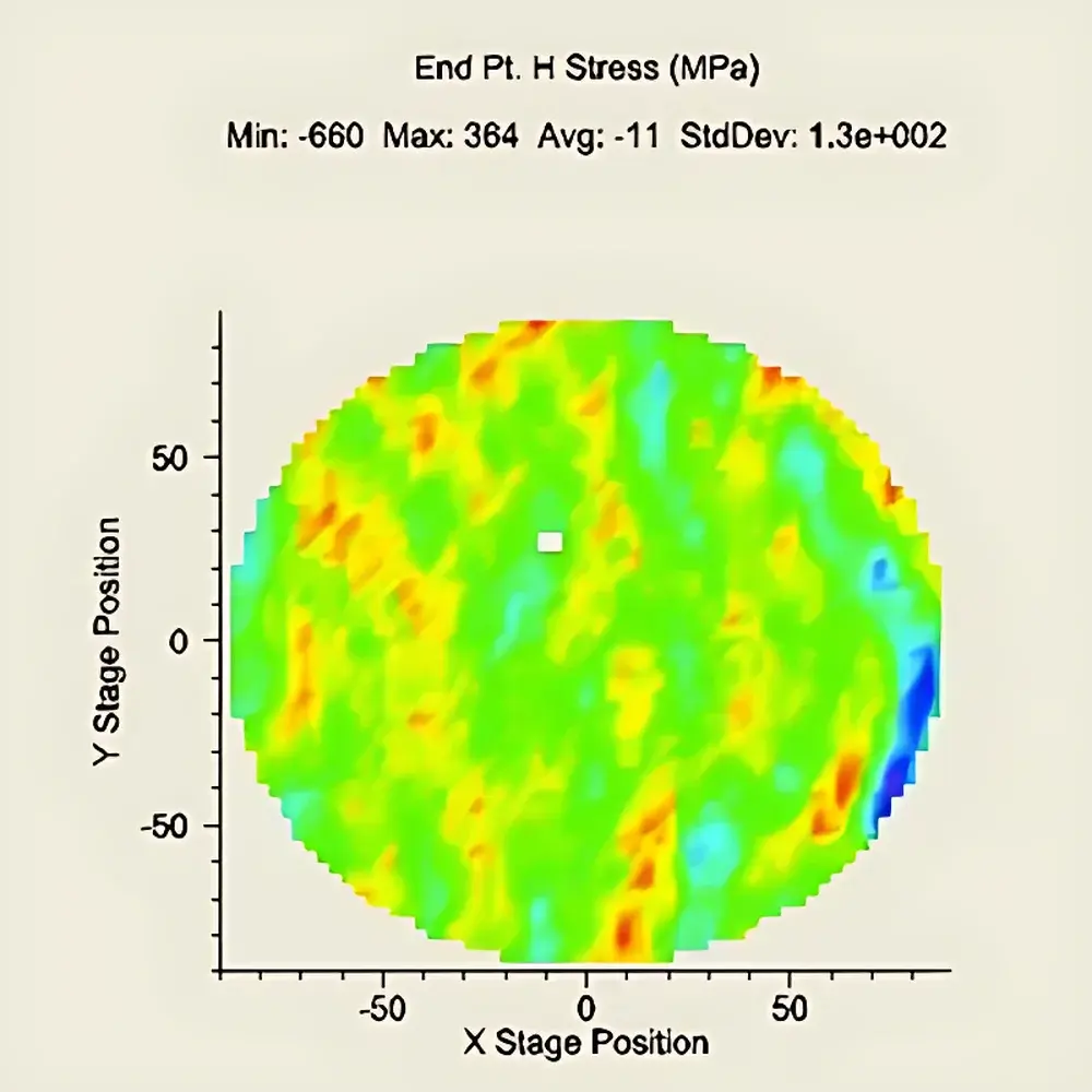
The kSA MOS UltraScan Thin Film Stress Tester is a high-precision, non-contact metrology system engineered for quantitative mechanical characterization of thin films on rigid substrates. It operates on the principle of multi-beam optical sensing (MOS), leveraging a two-dimensional laser array to measure surface slope gradients across a sample with sub-microradian sensitivity. By detecting minute changes in reflected beam angles across a dense grid of illumination points, the instrument reconstructs local surface curvature with nanometer-level vertical resolution. This curvature data—combined with substrate geometry, film thickness, and elastic modulus—is used to compute biaxial stress distribution via Stoney’s equation and its generalized formulations. Designed specifically for semiconductor process development and advanced optics manufacturing, the UltraScan delivers full-wafer 2D stress mapping at micron-scale spatial resolution, supporting both ambient and programmable temperature-controlled measurement environments.
Key Features
- Non-contact, vibration-insensitive MOS laser array architecture—eliminates mechanical probe artifacts and enables operation in shared lab environments without active isolation.
- Automated XY scanning platform with 1 µm step resolution and up to 20 mm/s scan velocity, supporting configurable scan patterns: region-of-interest, linear line scans, and full-area raster mapping.
- Simultaneous acquisition of mean curvature (1/R), curvature gradient, stress magnitude, stress anisotropy, and wafer-scale bow/warp metrics—all traceable to NIST-traceable interferometric calibration standards.
- Integrated thermal stage compatibility for in-situ stress vs. temperature profiling (e.g., coefficient of thermal expansion mismatch analysis), with programmable ramp rates and dwell control.
- Real-time optical tracking subsystem maintains beam alignment during extended scans, compensating for thermal drift and minor mechanical settling without user intervention.
- Ruggedized optical bench design with sealed beam paths and temperature-stabilized detectors ensures long-term measurement stability and inter-laboratory reproducibility.
Sample Compatibility & Compliance
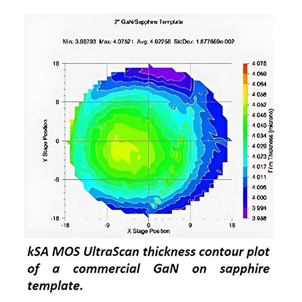
The kSA MOS UltraScan accommodates standard semiconductor wafers (up to 300 mm diameter), polished optical substrates (fused silica, CaF₂, BK7), glass panels, MEMS test chips, and coated lens elements. Surface finish requirements are consistent with ISO 10110–7 specifications (Rq < 5 nm). The system complies with ISO/IEC 17025 calibration traceability frameworks and supports audit-ready documentation for GLP and GMP environments. Data acquisition workflows adhere to FDA 21 CFR Part 11 principles through optional electronic signature and audit trail modules. All stress calculations follow ASTM F390-22 (Standard Test Method for Measuring Residual Stress in Thin Films by Curvature Measurements) and ISO 7640:2017 (Optics and photonics — Measurement of stress in thin films on substrates).
Software & Data Management
Control and analysis are performed via kSA’s proprietary UltraScan Studio software suite, built on a modular Qt-based architecture with Python API support. The interface provides real-time visualization of curvature maps, stress vector fields, and cross-sectional profiles. Quantitative outputs include ASCII and HDF5 export formats compatible with MATLAB, Python (NumPy/Pandas), and JMP for statistical process control (SPC). Built-in tools support spatial filtering, outlier suppression, substrate flatness correction, and multilayer stress deconvolution using iterative finite-element modeling. Software validation packages—including IQ/OQ documentation templates and version-controlled release notes—are provided for regulated environments.
Applications
- Process qualification of PVD, CVD, ALD, and epitaxial growth steps in front-end semiconductor fabrication.
- Thermal stress characterization of heterogeneous stacks (e.g., SiN/SiO₂/TiN) under controlled heating/cooling cycles.
- Defect correlation studies linking localized stress anomalies to particle contamination, edge chipping, or pattern density effects.
- Optical component certification—measuring figure error evolution in mirror substrates after coating deposition.
- MEMS packaging reliability assessment, including stress-induced delamination and hermetic seal integrity evaluation.
- Academic research in strain-engineered 2D materials, ferroelectric heterostructures, and flexible electronics substrate interactions.
FAQ
What substrate geometries and sizes does the UltraScan support?
Standard configurations accommodate flat, circular substrates from 50 mm to 300 mm in diameter; custom stages are available for rectangular optics up to 200 × 200 mm.
Can the system measure stress during deposition?
No—the UltraScan is a post-process ex-situ tool. For in-situ monitoring, k-Space offers the kSA MOS Film Stress Tester designed for integration into MBE, sputter, and CVD chambers.
Is calibration required between measurements?
The system performs automated reference calibration at startup and before each scan sequence using internal fiducial targets; no manual recalibration is needed under normal operating conditions.
How is film thickness incorporated into stress calculation?
Users input nominal film thickness and Young’s modulus either manually or via CSV import; optional integration with ellipsometry or XRR tools enables automated parameter chaining.
Does the software support automated pass/fail reporting per industry SPC limits?
Yes—customizable rule sets can trigger alerts, generate PDF reports, and export results to MES or LIMS platforms via OPC UA or RESTful API interfaces.
Related Products


