
Lithography & Coating/Developing Equipment
Filter
Showing 61–90 of 114 results
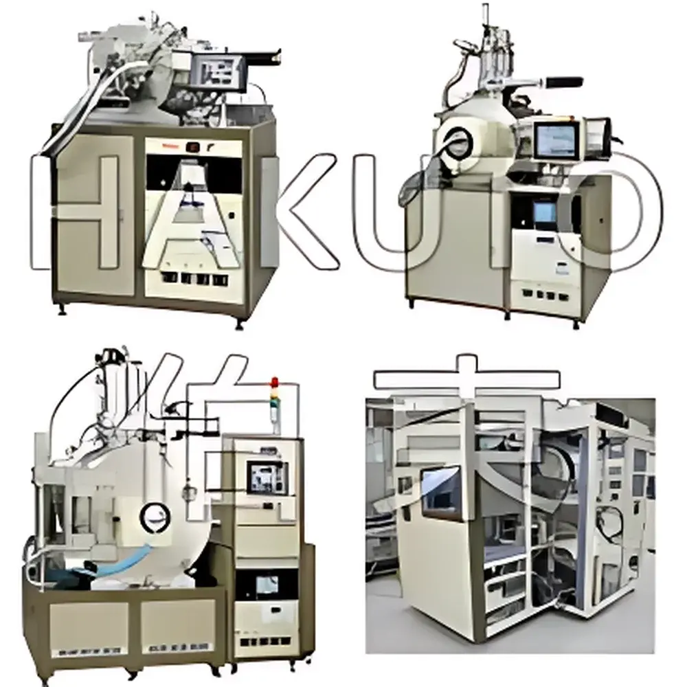
| Brand | NS (Nippon Seiko) |
|---|---|
| Origin | Japan |
| Manufacturer Type | Authorized Distributor |
| Origin Category | Imported |
| Model | IBE |
| Price Range | USD 210,000 – 280,000 |
| Sample Diameter | 3"–6" φ |
| Max. Ion Incidence Angle | ±90° |
| Ion Source | Kaufman-type KDC-40 / KDC-75 / KDC-160 (KRI, USA) |
| Ultimate Vacuum | ≤1×10⁻⁴ Pa (4IBE/7.5IBE/16IBE/20IBE), ≤8×10⁻⁵ Pa (MEL 3100) |
| Turbomolecular Pump | Pfeiffer (350 L/s or 1250 L/s) |
| Etch Uniformity | ≤±5% |
| Cooling | Direct substrate cooling |
| Motion System | Dry Chuck Planet (planetary rotation + revolution) |
| Etch Mode | Physical sputtering (Ar⁺ beam), non-reactive, anisotropic |
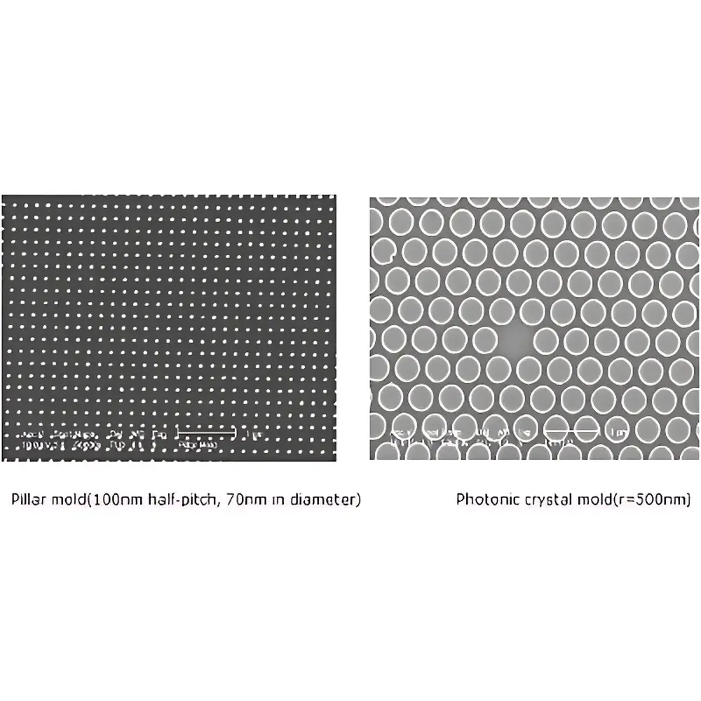
| Origin | Jiangsu, China |
|---|---|
| Manufacturer Type | Authorized Distributor |
| Origin Category | Domestic |
| Model Variants | Quartz / Silicon / Polymer Templates |
| Pricing | Available Upon Request |
| Template Materials | Fused Silica (Quartz), Single-Crystal Silicon, Silicon Nitride (SiNₓ), Silicon Carbide (SiC), Borosilicate Glass |
| Max Template Diameter | 100 mm (4″) |
| Minimum Feature Size | 50 nm (for ≤2″ area) |
| EBL Service Capability | Down to 30 nm feature size |
| Substrate Compatibility | Conductive (e.g., Si, GaAs, InP) and Non-Conductive (e.g., SiO₂/Si, quartz, polymer-coated wafers) substrates |
| Fabrication Scope | Micro- and nanoscale patterning on Si, III–V (GaAs, InP), II–VI (ZnS, CdTe), and polymer substrates |
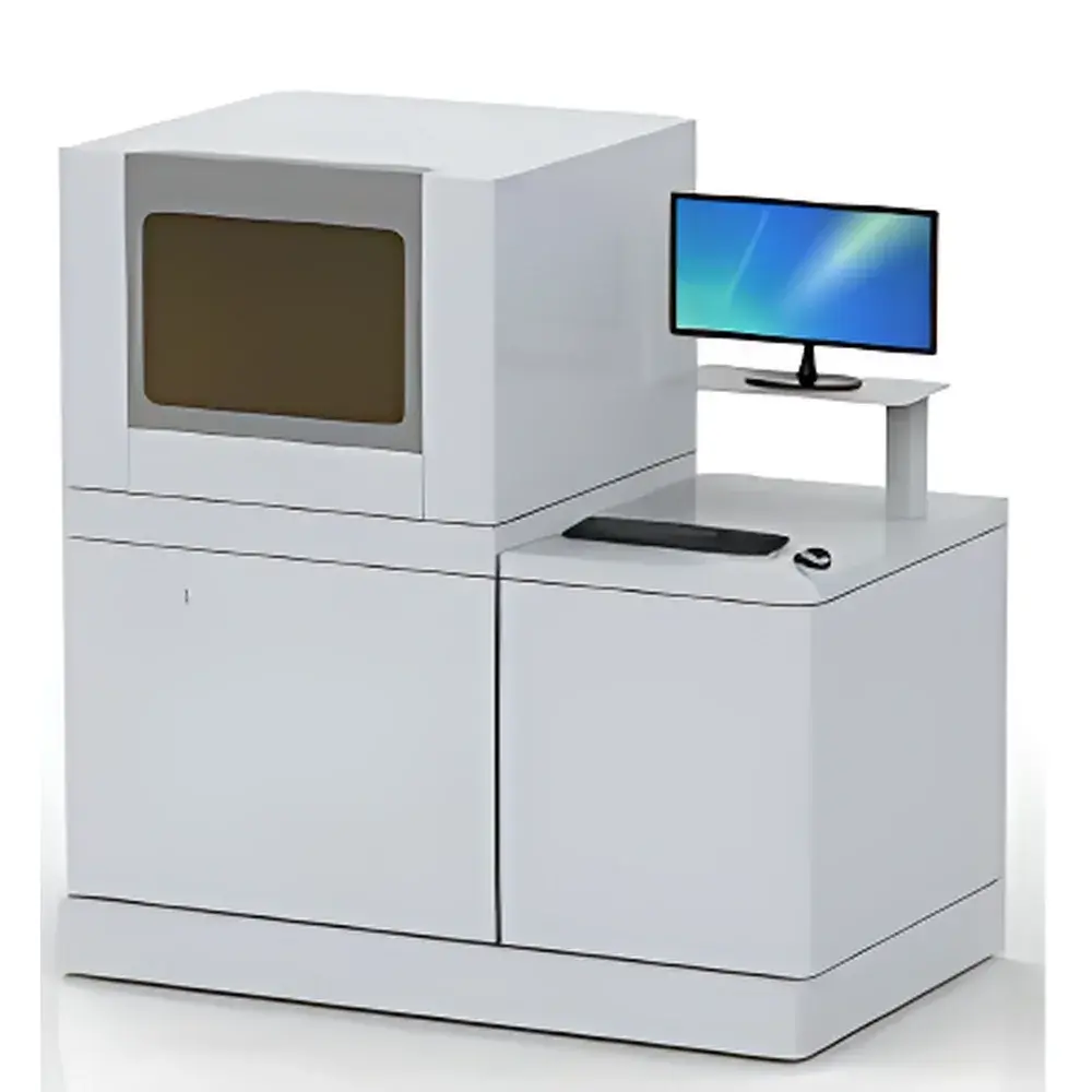
| Origin | Hong Kong |
|---|---|
| Manufacturer Type | Authorized Distributor |
| Origin Category | Mainland China Made |
| Model | Holimatrix |
| Price Range | USD 140,000 – 210,000 |
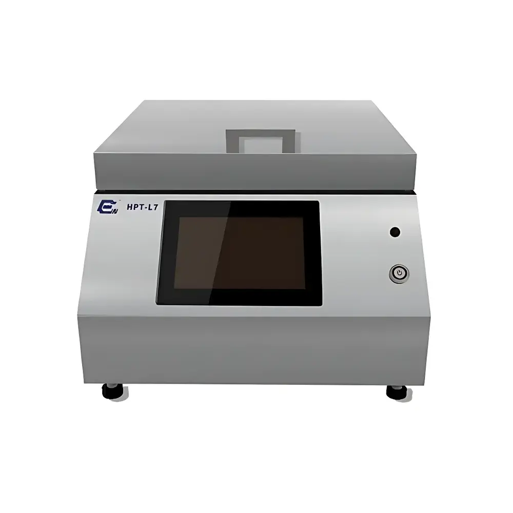
| Brand | EWIN-TECH |
|---|---|
| Origin | Shanghai, China |
| Manufacturer Type | OEM/ODM Manufacturer |
| Country of Origin | China |
| Model | HPT-L7 |
| Pricing | Upon Request |
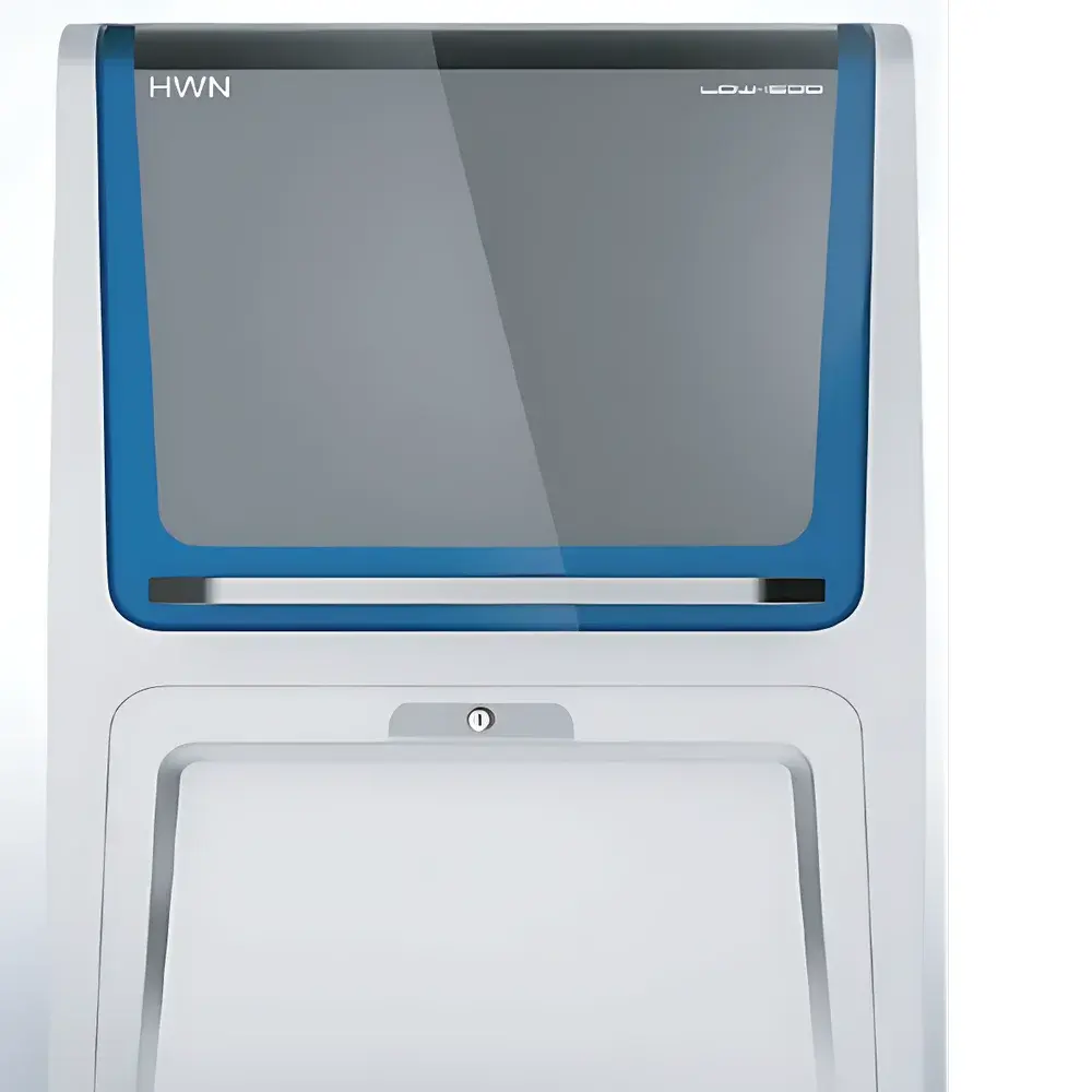
| Brand | Huaweina |
|---|---|
| Origin | Jiangsu, China |
| Manufacturer Type | Authorized Distributor |
| Product Origin | Domestic (China) |
| Model | LDW-P |
| Price Range | USD 14,000 – 28,000 |
| Maximum Writing Resolution | 50 nm |
| Minimum Spot Size | 275 nm |
| Minimum Grid Pitch | 75 nm |
| Stage Resolution | 1 nm |
| Absolute Positioning Accuracy | <10 nm |
| Writing Field Options | 100×100 to 1500×1500 µm |
| Laser Power Stability | <±1% RMS |
| Software Platform | LDW-SC Control Suite |
| Optical Principle | Nonlinear Threshold-Dependent Ablation/Modification via Gaussian-Focused Ultrafast Laser Pulses |
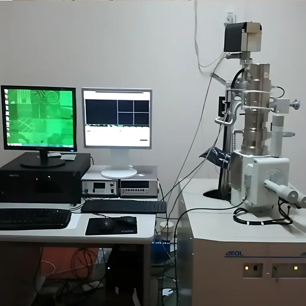
| Brand | JC Nabity |
|---|---|
| Origin | USA |
| Model | NPGS V9.2 |
| Minimum Feature Size | 10 nm |
| Electron Beam Diameter | ≤1 nm |
| Accelerating Voltage Range | 0–40 kV |
| Control Interface | PCIe-516A High-Speed Lithography Board |
| Host Compatibility | Commercial SEM, STEM, or FIB Systems |
| Operating System | Windows 10 |
| Pattern Design Software | QCAD |
| Beam Blanking Frequency | Up to 5 MHz |
| Brand | JEOL |
|---|---|
| Origin | Japan |
| Model | JBX-9500FS |
| Acceleration Voltage | 100 kV |
| Maximum Substrate Size | 300 mm Ø wafers or 6-inch masks |
| Maximum Field Size | 1000 µm × 1000 µm |
| Stage Travel Range | 260 mm × 240 mm |
| Minimum Positioning Unit (LBC) | 0.15 nm (λ/4096) |
| Overlay Accuracy | ≤ ±11 nm |
| Field Stitching Accuracy | ≤ ±10 nm |
| In-Field Placement Accuracy | ≤ ±9 nm |
| Position DAC Resolution | 20-bit |
| Scan DAC Resolution | 14-bit |
| Scan Step Size | 0.25 nm |
| Maximum Scan Rate | 100 MHz |
| Electron Source | ZrO/W Schottky Emitter |
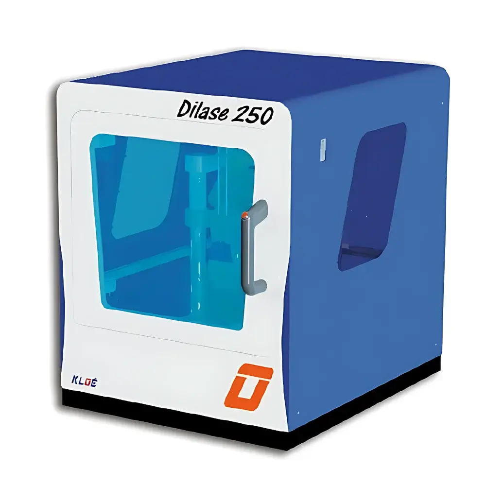
| Brand | KLOE |
|---|---|
| Origin | France |
| Model | Dilase 250 |
| Exposure Mode | Non-contact (Flying Spot) |
| Resolution | ≤100 nm (line width, under optimal resist & process conditions) |
| Wavelength | 375 nm or 405 nm (solid-state laser) |
| Beam Spot Size | Adjustable from 1 µm to 50 µm |
| Writing Area | 100 mm × 100 mm |
| Stage Positioning Accuracy | 100 nm (standard), 40 nm (optional) |
| Repeatability | ±100 nm |
| Overlay Accuracy (Multi-layer) | ≤1 µm |
| Orthogonality Error | <1 mrad |
| Maximum Sample Size | Up to 125 mm square (5-inch equivalent) |
| Substrate Thickness Range | 250 µm – 5 mm |
| Laser Lifetime | >10,000 h |
| File Format Support | GDSII, OASIS, DXF, LWO |
| Safety Compliance | EN 60825-1, IEC 61000-6-2/6-4, CE Marked |
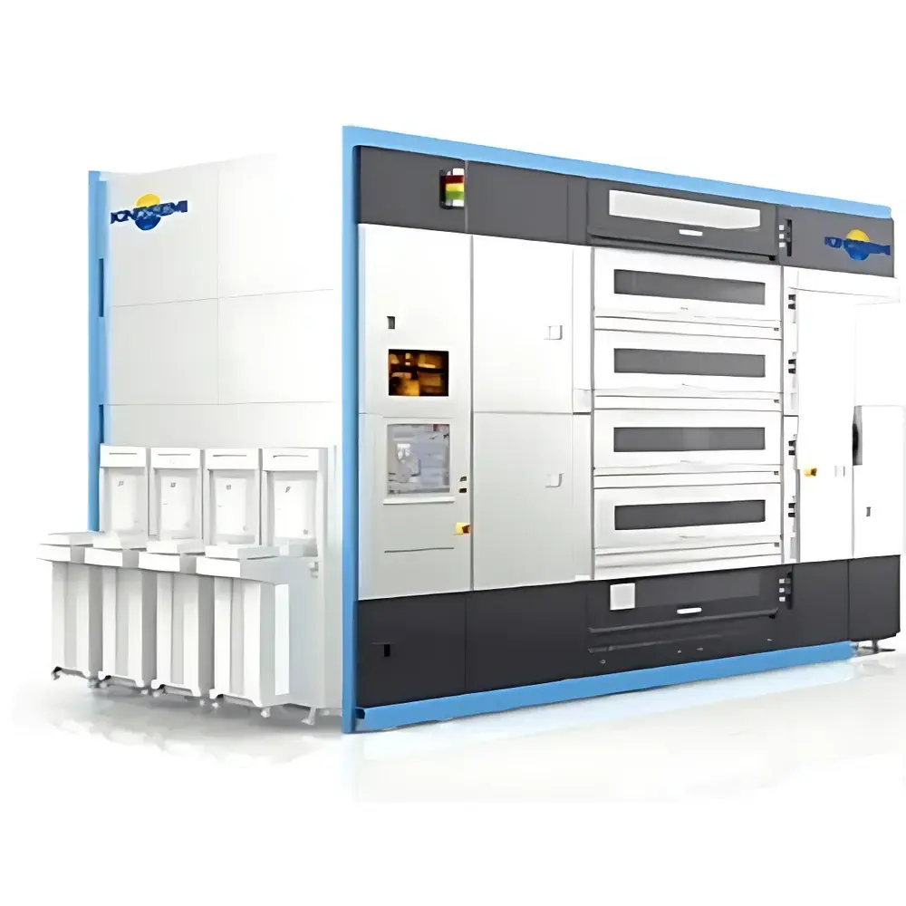
| Brand | Kingsemi |
|---|---|
| Origin | Liaoning, China |
| Model | KS-FT200/300 (8"/12" Front-End Process) |
| Application | ArF/KrF/I-Line photoresists, PI, BARC, SOC, SOD, SOG |
| Integration | Compatible with track-to-scanner inline lithography systems |
| Certification | Compliant with SEMI S2/S8 safety standards, ISO 14644-1 Class 5 cleanroom operation |
| Architecture | Modular stackable design |
| Thermal Control | Optional high-precision hot/cold plates (±0.1°C uniformity) |
| Inspection | Optional integrated Wafer Edge Exposure (WEE) and Automated Optical Inspection (AOI) modules |
| Maintenance | Front-accessible modular units with tool-less panel removal |
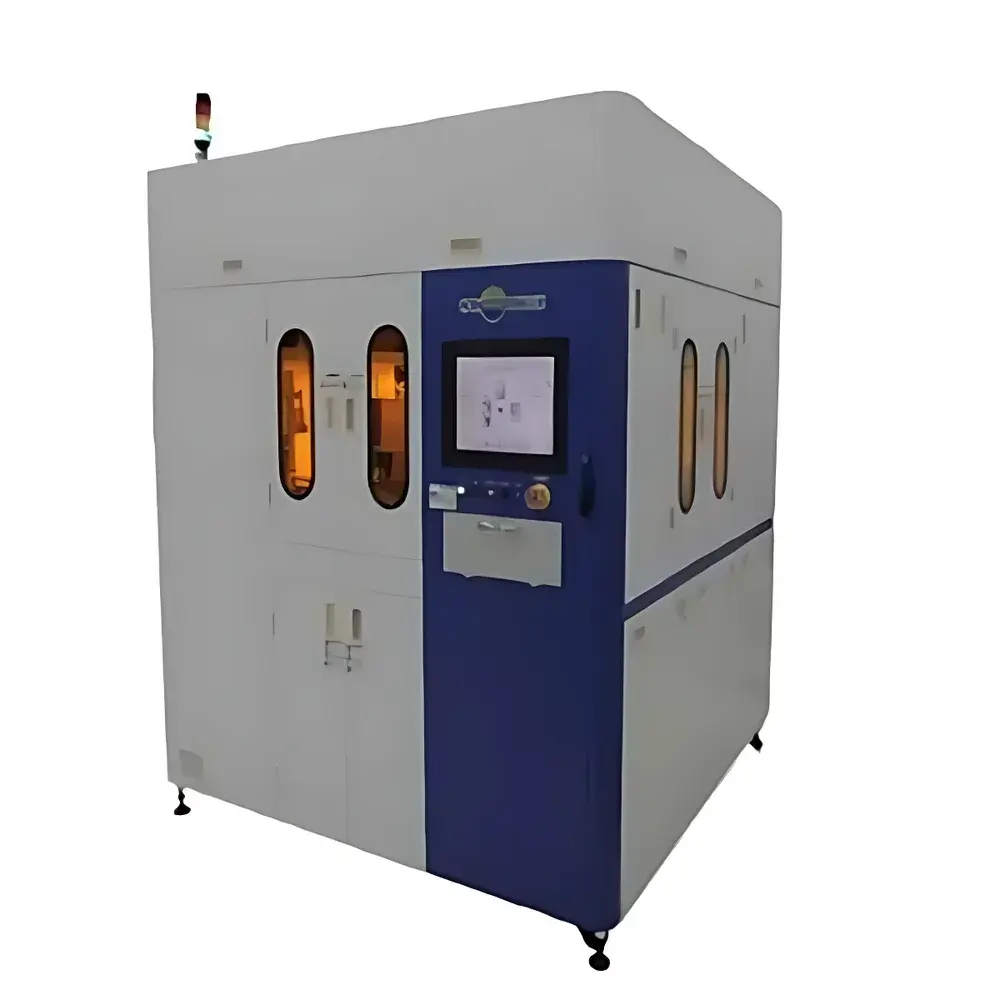
| Brand | Kingsemi |
|---|---|
| Model | KS-S150 |
| Configuration | Star-type fully automated coater/developer |
| Substrate Compatibility | Sapphire, GaAs, SiC wafers (4", 6") |
| Throughput | ≥190 wafers/hour (coating module) |
| Photoresist Consumption | 0.6 mL per 4" wafer |
| Certification | CSA Certified |
| Origin | Liaoning, China |
| Equipment Type | Semiconductor Coater/Developer for Patterning Processes |
| Application Scope | LED-PSS, compound semiconductor fabrication, sensor ICs, optical communication chips, power devices, patterned sapphire substrates |
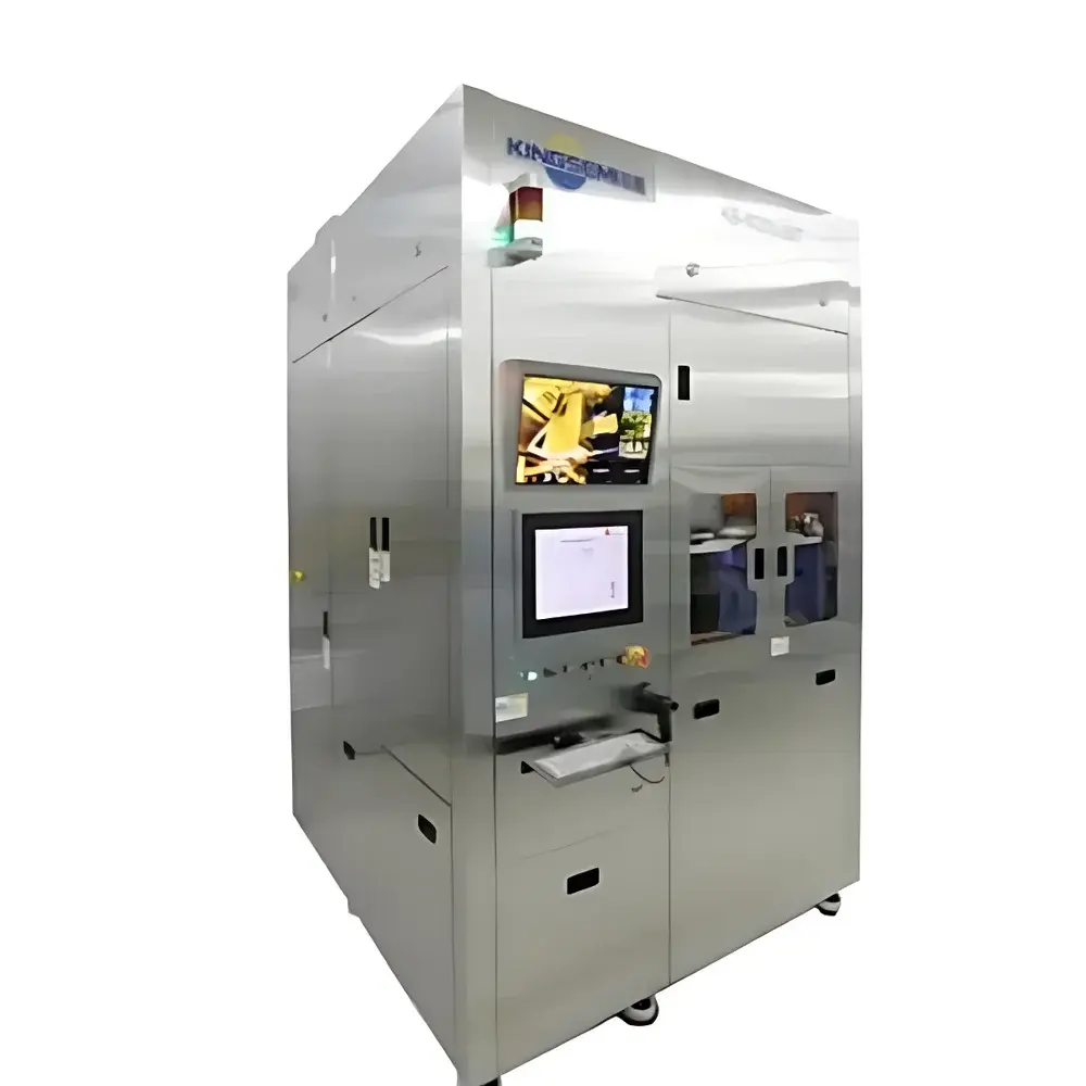
| Brand | Kingsemi |
|---|---|
| Model | KS-S150-6ST |
| Origin | Liaoning, China |
| Equipment Type | Semiconductor Resist Stripping System |
| Configuration | 6-Station Wet Processing Platform |
| Vacuum Handling | Dual-Vacuum Dual-Clamp High-Speed Robotic Arm |
| Alignment | Automated Wafer Centering (AWC) with Vision-Based Recognition |
| Bath Compatibility | Multi-Size & Multi-Angle Immersion Modules (150 mm to 200 mm wafers) |
| Pressure Control | Closed-Loop High-Pressure Fluid Delivery (±0.2 MPa accuracy) |
| Heating System | In-Line High-Pressure Resistant Heater (PID-controlled, ≤120 °C) |
| Chuck Type | Actively Clamped, Backside-Protected Electrostatic/ Mechanical Chuck |
| Chemical Recovery | Integrated Solvent Recovery and Recirculation Loop |
| Compliance | Designed for Class 100 Cleanroom Integration |
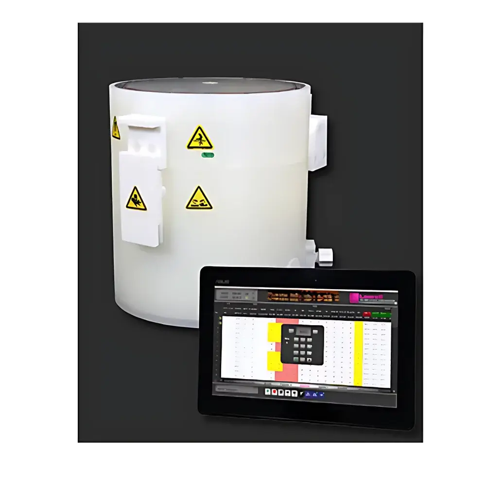
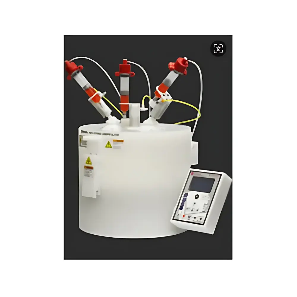
| Brand | Laurell |
|---|---|
| Origin | USA |
| Model | H6-15 |
| Maximum Speed | 12,000 rpm (at 100 mm Si wafer) |
| Substrate Compatibility | up to 300 mm wafers and 9″ × 9″ (229 mm × 229 mm) square substrates |
| Control Interface | Wireless tablet with Laurell Touch software |
| Firmware Upgradability | Field-upgradable via downloadable updates |
| Software | Spin3000 PC-based process management suite (free, includes virtual simulation mode) |
| Enclosure Compatibility | Designed for integration into gloveboxes |
| Modular Expansion | Field-upgradable via plug-in modules |
| Compliance | Supports GLP/GMP traceability requirements through audit-ready process logging |
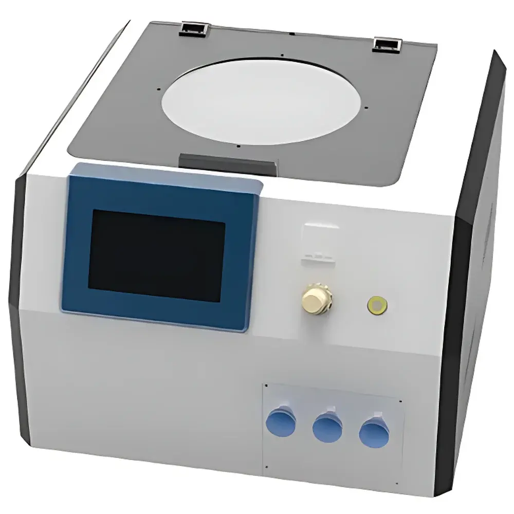
| Brand | Laurell |
|---|---|
| Origin | USA |
| Model | WS-650-8B |
| Maximum Substrate Size | 200 mm wafer or 178 mm × 178 mm square substrate |
| Max Speed | 12,000 rpm (at 100 mm Si wafer) |
| Controller | 650 Series Microprocessor-Based Process Controller |
| Software | Spin3000 PC Control & Simulation Suite (free, optional but fully compatible) |
| Housing Material | Chemically resistant solid copolymer blend (standard) or PTFE Hostaflon® TFM-1600 / Teflon® AF (optional, high-temp/ultra-clean) |
| Sealing | Proprietary labyrinth seal with N₂ purge capability |
| Compliance | Designed for ISO Class 5–4 cleanroom integration |
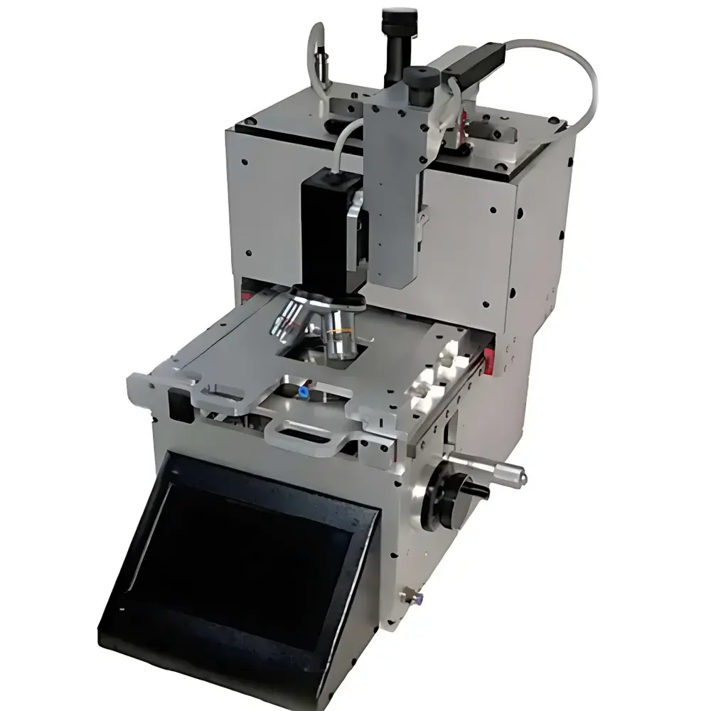
| Brand | LEBO Science |
|---|---|
| Origin | Imported |
| Manufacturer Type | Authorized Distributor |
| Model | Customized-2 |
| Wafer Compatibility | Fragments to 200 mm (customizable up to 300 mm with quad-nozzle configuration) |
| Development Modes | Single-step & Multi-step Programmable Process |
| Max. Spin Speed | 3000 rpm (no-load) |
| Speed Resolution | ±1 rpm |
| Acceleration Range | 10–10,000 rpm/sec (no-load) |
| Step Duration Range | 0–3000 sec |
| Time Resolution | 0.1 sec |
| Nozzle Control | Motorized XYZ-positioning with programmable trajectory |
| Fluid Delivery | 1 dedicated developer channel + 1 deionized water rinse channel + 1 N₂ purge channel |
| Compliance | Designed for Class 100–1000 cleanroom environments |
| Software | Onboard HMI with 100 user-editable process recipes |
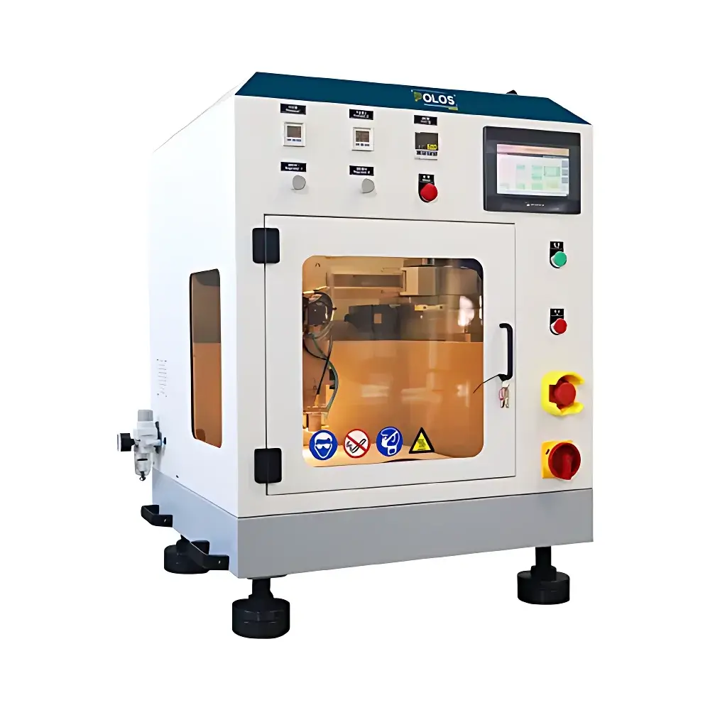
| Brand | Makeway |
|---|---|
| Origin | USA |
| Model | MKW-280 |
| Mask Size | 5 in |
| Wafer/Substrate Size | 5 in |
| Alignment Accuracy | 1 µm (Vacuum Contact), 1.5 µm (Hard Contact), 3 µm (Soft Contact), 5 µm (Proximity Mode) |
| UV Source | 350 W, 365 nm, uniformity ±3%, irradiance 30 mW/cm² |
| Exposure Time Range | 0.1–999 s |
| Chuck Motion | Manual X/Y/Z/θ with wedge compensation leveling |
| Microscopy | Dual CCD-based system, 80×–400× standard, up to 1000× with optional lenses, working distance 50–150 mm |
| Display | 20" LCD monitor |
| Contact Modes | Vacuum contact (adjustable force), hard contact, soft contact, proximity (gap adjustable) |
| Power Supply | 220 V, single-phase, 15 A |
| Optional | Deep UV source, IR alignment mode, custom substrate chucks |
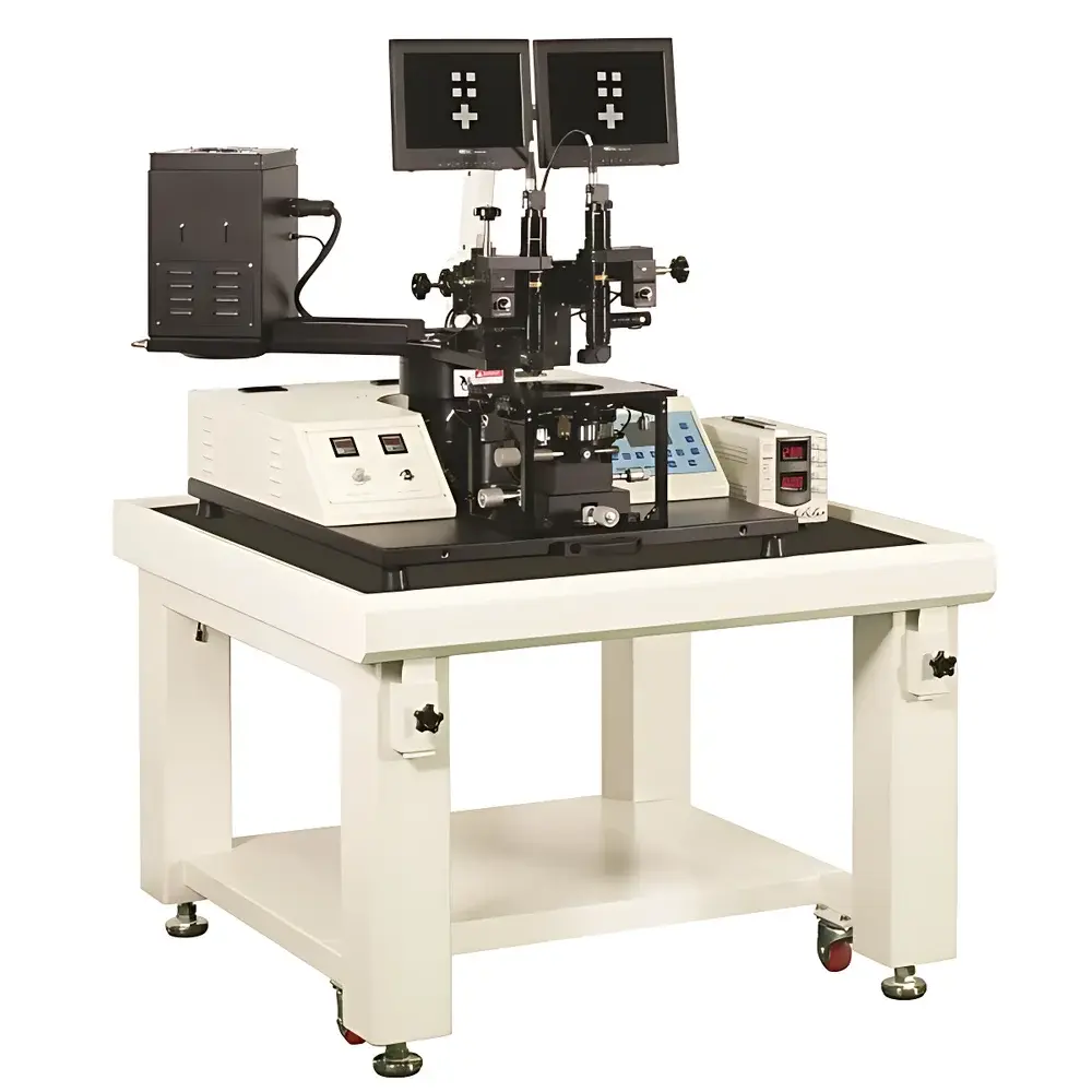
| Brand | Makeway |
|---|---|
| Origin | Shanghai, China |
| Manufacturer Type | Authorized Distributor |
| Region of Origin | Domestic (China) |
| Model | MKW-320 |
| Price Range | USD 21,000 – 55,000 |
| Brand | Midas |
|---|---|
| Origin | South Korea |
| Manufacturer Status | Authorized Distributor |
| Origin Category | Imported |
| Model | MDA-400LJ |
| Pricing | Upon Request |
| Mask Size Max | 5-inch |
| Substrate Size Max | 4-inch circular wafers |
| Beam Shape | Circular |
| Beam Diameter | 125 mm |
| Light Source | UV LED |
| Wavelength | 365 nm |
| Beam Uniformity | < ±3 % |
| Peak Irradiance at 365 nm | 25 mW/cm² |
| Alignment Method | Manual |
| Alignment Accuracy | ±1 µm |
| Exposure Modes | Soft Contact, Hard Contact, Proximity (Vacuum-assisted) |
| Resolution | 1 µm (with 1 µm photoresist thickness under vacuum contact) |
| Weight | 150 kg |
| Dimensions (W×D×H) | 995 × 800 × 850 mm |
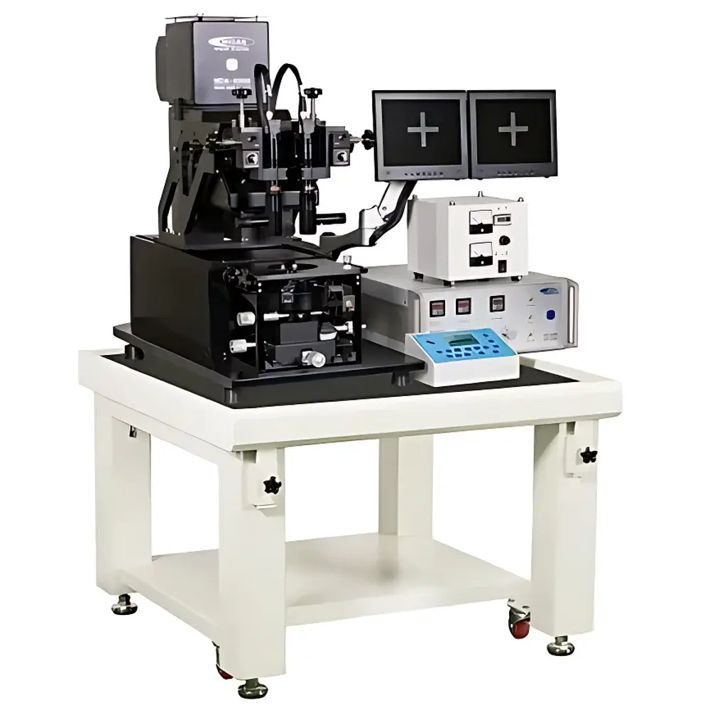
| Brand | MIDAS |
|---|---|
| Origin | South Korea |
| Model | MDA-400M |
| Exposure Source | Ushio 350W UV Lamp (or optional 365 nm LED, 10,000 h lifetime) |
| Resolution | 1 µm (vacuum/hard contact), 2 µm (soft contact), 5 µm (20 µm gap proximity) |
| Beam Size | 4.25 × 4.25 inch |
| Uniformity | ≤3% (over 4-inch field) |
| Intensity | >30 mW/cm² @ 365 nm |
| Exposure Time | 0.1–999.9 s |
| Alignment Accuracy | ±0.5 µm |
| Stage Travel | X/Y ±10 mm, θ ±5°, Z ±10 mm |
| Approach Step Resolution | 1 µm |
| Microscopy | Dual CCD zoom microscope (80×–480×), 17″ LCD monitor |
| Substrate Compatibility | 2″, 3″, 4″ wafers |
| Mask Size | 4″ and 5″ |
| Vacuum Requirement | < −200 mbar (integrated oil-free pump) |
| CDA | >5 kg/cm² |
| N₂ | >3 kg/cm² |
| Power | 220 V, 15 A, single-phase |
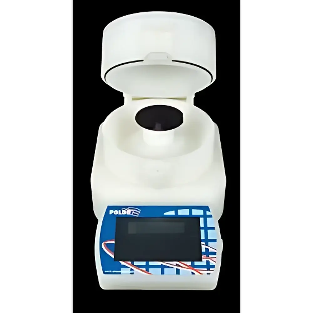
| Brand | Midas |
|---|---|
| Origin | Germany |
| Model | SPIN150X |
| Max. Rotation Speed | 12000 rpm |
| Speed Accuracy | ±1 rpm |
| Max. Acceleration | 30000 rpm/s |
| Substrate Diameter | up to 160 mm (6") |
| Chamber Diameter | 202 mm |
| Controller Memory | 50 programs × 99 steps each |
| Programmable Outputs | 2 dry-contact relays |
| Dimensions (W×D×H) | 275 × 240 × 450 mm |
| Housing Material | Natural Polypropylene (NPP) or PTFE options |
| Sample Compatibility | 5 mm to 160 mm round wafers or 4" × 4" square substrates |
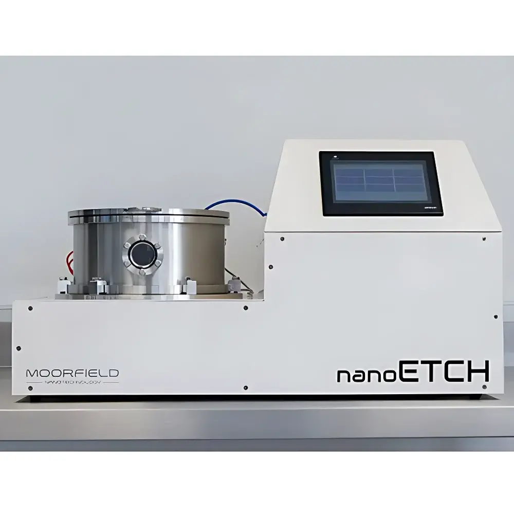
| Brand | Moorfield |
|---|---|
| Origin | United Kingdom |
| Model | nanoETCH |
| RF Power Range | <30 W (milliwatt-resolution control) |
| Base Pressure | <5×10⁻⁷ mbar |
| Sample Stage Options | 3-inch & 6-inch |
| Vacuum System | Turbomolecular pump with optional backing pump |
| Gas Delivery | Mass Flow Controller (MFC)-regulated |
| Control Interface | Integrated touchscreen HMI with programmable etch recipes |
| Data Logging | PC-compatible USB/Ethernet interface |
| Safety Compliance | CE, IEC 61000-6-4, IEC 61000-6-2 |
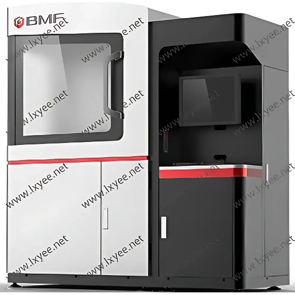
| Origin | USA |
|---|---|
| Manufacturer Type | Authorized Distributor |
| Origin Category | Imported |
| Model | P130 / S130 |
| Price Range | USD 280,000 – 420,000 |
| UV Light Source | 405 nm LED |
| XY Resolution | 2–10 µm |
| Layer Thickness | 5–20 µm |
| Build Volume (P130) | 3.84 × 2.16 × 10 mm (Mode 1) / 38.4 × 21.6 × 10 mm (Mode 2) / 50 × 50 × 10 mm (Mode 3) |
| Build Volume (S130) | Up to 100 × 100 × 50 mm |
| Optical System | High-NA Projection Micro-Lithography Optics |
| Post-Processing | Integrated Vacuum Despersion + UV Curing Station |
| Power Requirement | 200–240 V AC, 50/60 Hz, 3 kW |
| Weight | 450 kg |
| Dimensions | 1720 × 650 × 1820 mm |
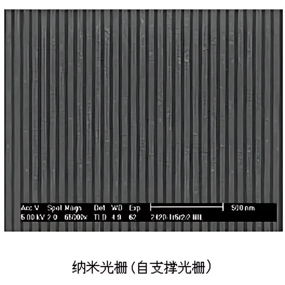
| Origin | Jiangsu, China |
|---|---|
| Manufacturer Type | Authorized Distributor |
| Regional Origin | Domestic (PRC) |
| Model | Custom Grating Fabrication |
| Pricing | Available Upon Technical Consultation |
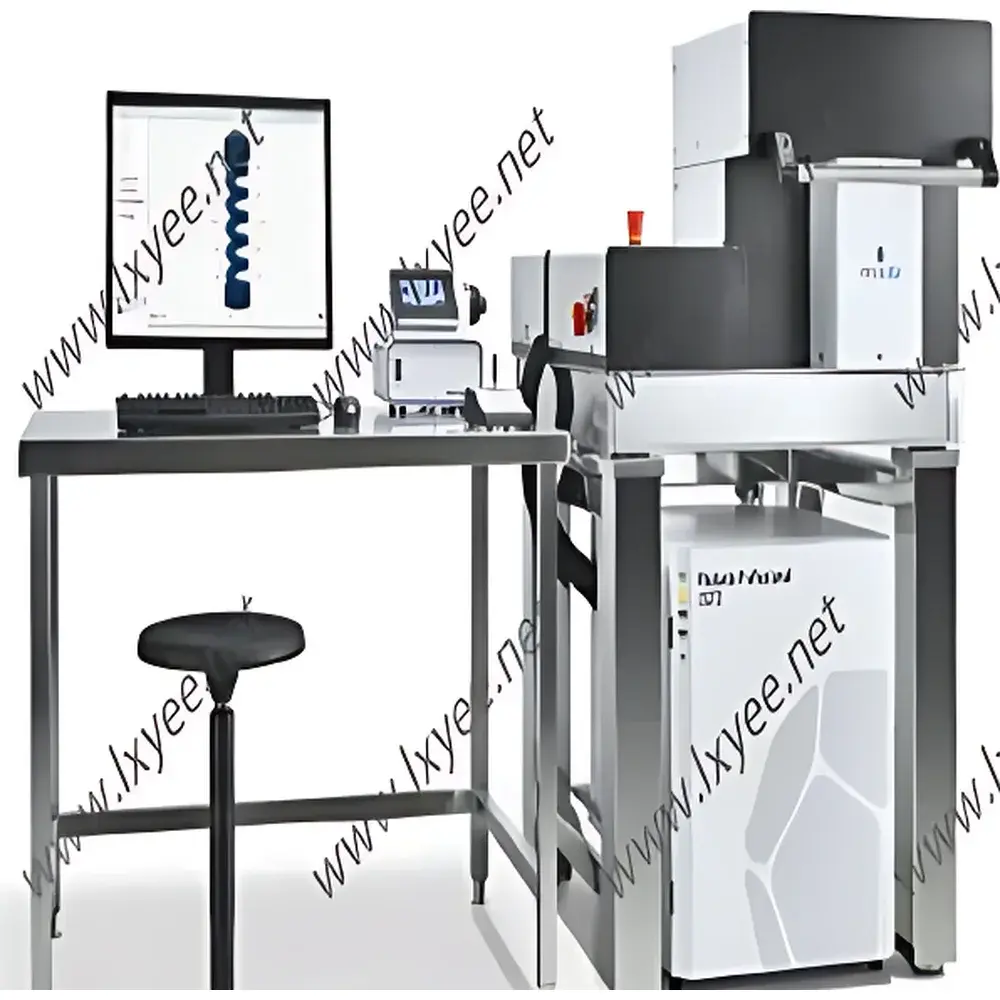
| Brand | Nanoscribe |
|---|---|
| Country of Origin | Germany |
| Model | Photonic Professional GT2 |
| Category | Two-Photon Polymerization (TPP) Microfabrication System |
| Automation Level | Fully Automated |
| User Interface | Intuitive Graphical Workflow Environment |
| Compliance Framework | Designed for ISO 14644-1 Class 5 cleanroom integration |
| Software Architecture | Windows-based, FDA 21 CFR Part 11–ready audit trail support (optional configuration) |
| Brand | Nanoscribe |
|---|---|
| Origin | Germany |
| Manufacturer Type | Authorized Distributor |
| Origin Category | Imported |
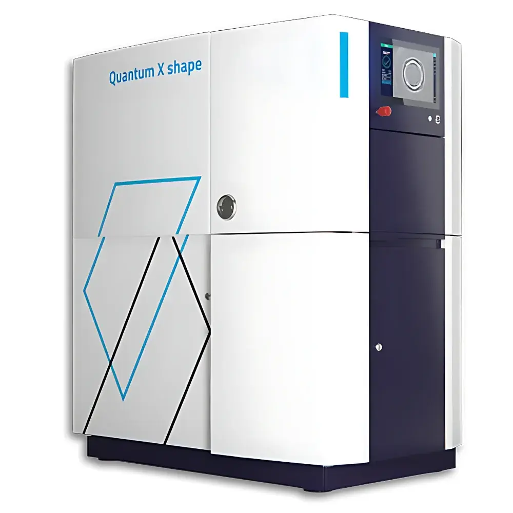
| Model | Quantum X shape |
| Exposure Mode | Proximity-Based Two-Photon Absorption |
| Resolution | 100 nm (feature size) |
| Light Source | Femtosecond Pulsed Near-Infrared Laser |
| Wavelength | 780 nm |
| Intensity Uniformity | ±1% |
| Maximum Exposure Area | 100 mm diameter |
| Surface Roughness (Ra) | ≤ 5 nm |
| Shape Accuracy | ≤ 200 nm |
| Single Print Field Diameter | ≥ 4,000 µm |
| Max Scanning Speed | 6.25 m/s (at 10× objective) |
| Substrate Compatibility | Up to 200 mm (8″) wafers, glass, silicon, opaque substrates |
| Compatible Photoresists | Nanoscribe IP-series (polymer), GP-Silica (glass-like), and third-party resists |
| Brand | NILT |
|---|---|
| Origin | Denmark |
| Manufacturer Type | Authorized Distributor |
| Origin Category | Imported |
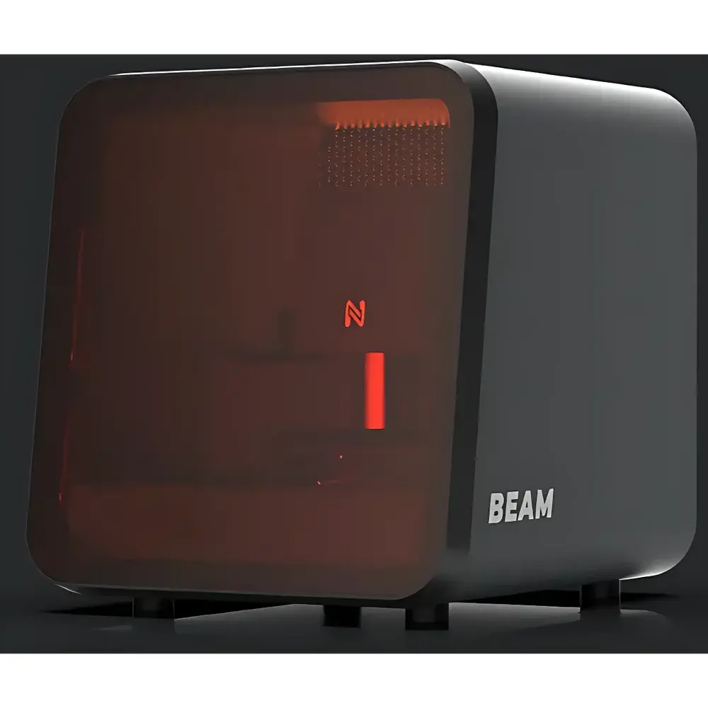
| Model | BEAM |
| Exposure Mode | Proximity-style Direct Write |
| Resolution | ≤500 nm (line width) |
| Light Source | UV Diode Lasers |
| Wavelengths | 365 nm, 385 nm, 405 nm |
| Illumination Uniformity | Optimized via Dynamic Beam Shaping & Real-time Power Calibration |
| Exposure Field | 106 mm × 106 mm or 150 mm × 150 mm (tileable) |
| Autofocus Speed | <1 s (piezo-driven closed-loop Z-control) |
| Pattern Writing Speed | <2 s per 10 mm × 10 mm field (at 500 nm resolution, AZ5214E resist) |
| Maximum Substrate Size | 6-inch (150 mm) wafers or square substrates up to 150 mm × 150 mm |
| Alignment Accuracy | <±200 nm (multi-layer, vision-based auto-alignment) |
| Software Interface | GDSII-native workflow with real-time pattern preview, tile stitching, and wafer-level navigation |
| Brand | NILT |
|---|---|
| Origin | Imported |
| Manufacturer Type | Authorized Distributor |
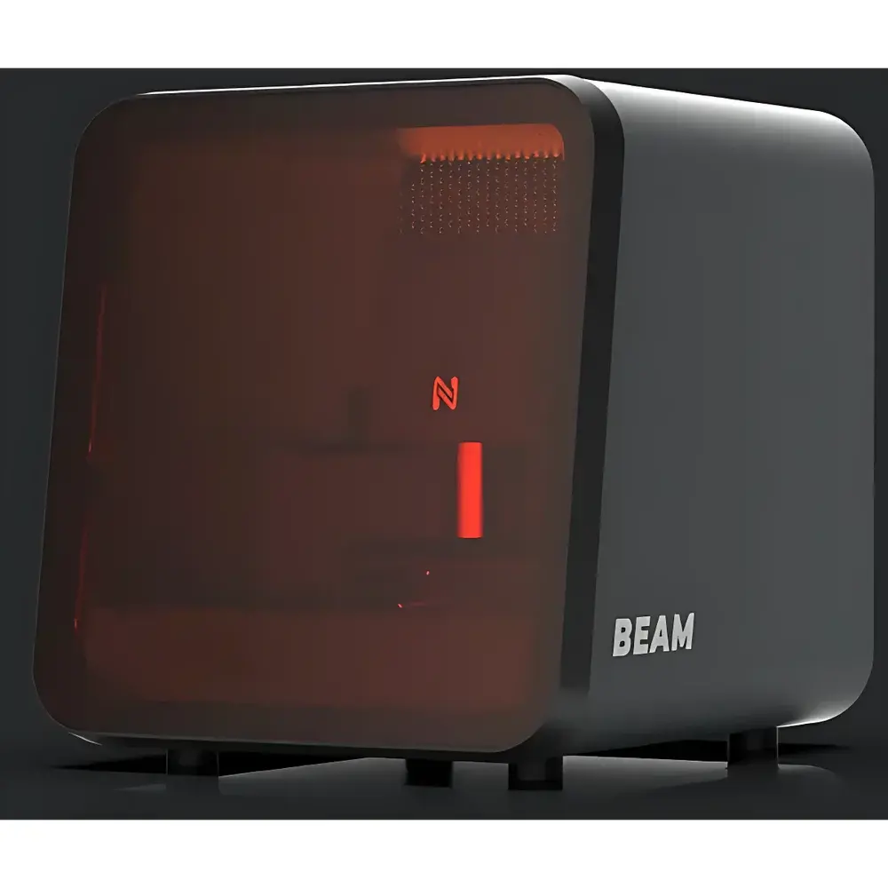
| Exposure Mode | Proximity |
| Resolution | 500 nm |
| Light Source | UV Laser |
| Wavelengths | 405 nm, 365 nm, 385 nm |
| Illumination Uniformity | Direct-write scanning mode |
| Maximum Exposure Area | 150 mm × 150 mm |
| Compatible Substrate Sizes | Up to 6-inch wafers |
| Autofocus Speed | <1 s (piezo-driven closed-loop optical focus control) |
| Pattern Writing Speed | <2 s per defined exposure field |
| Alignment Method | Semi-automated multi-layer alignment with real-time image recognition |
| Software Interface | GDSII-compatible, CNC-style navigation (WASD), on-the-fly pattern placement, wafer-level map visualization |
| Brand | NILT |
|---|---|
| Origin | Denmark |
| Manufacturer Type | Authorized Distributor |
| Origin Category | Imported |
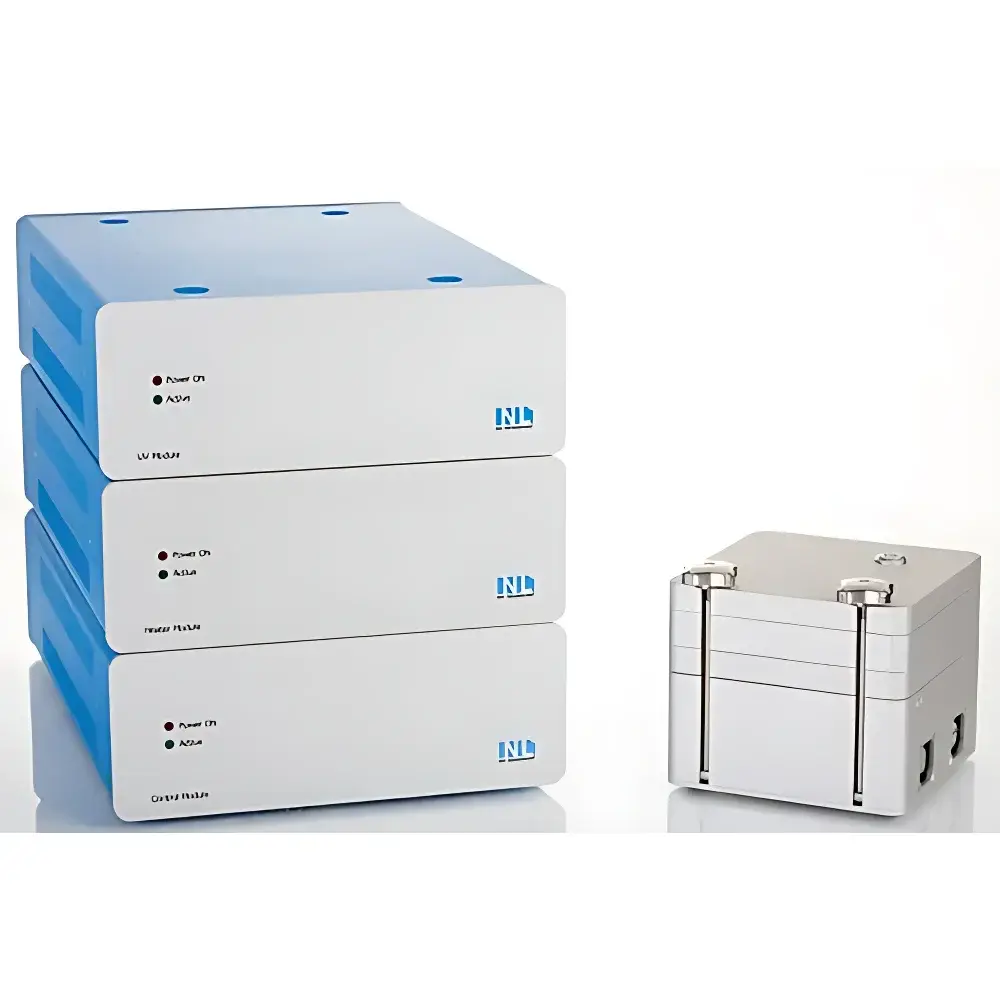
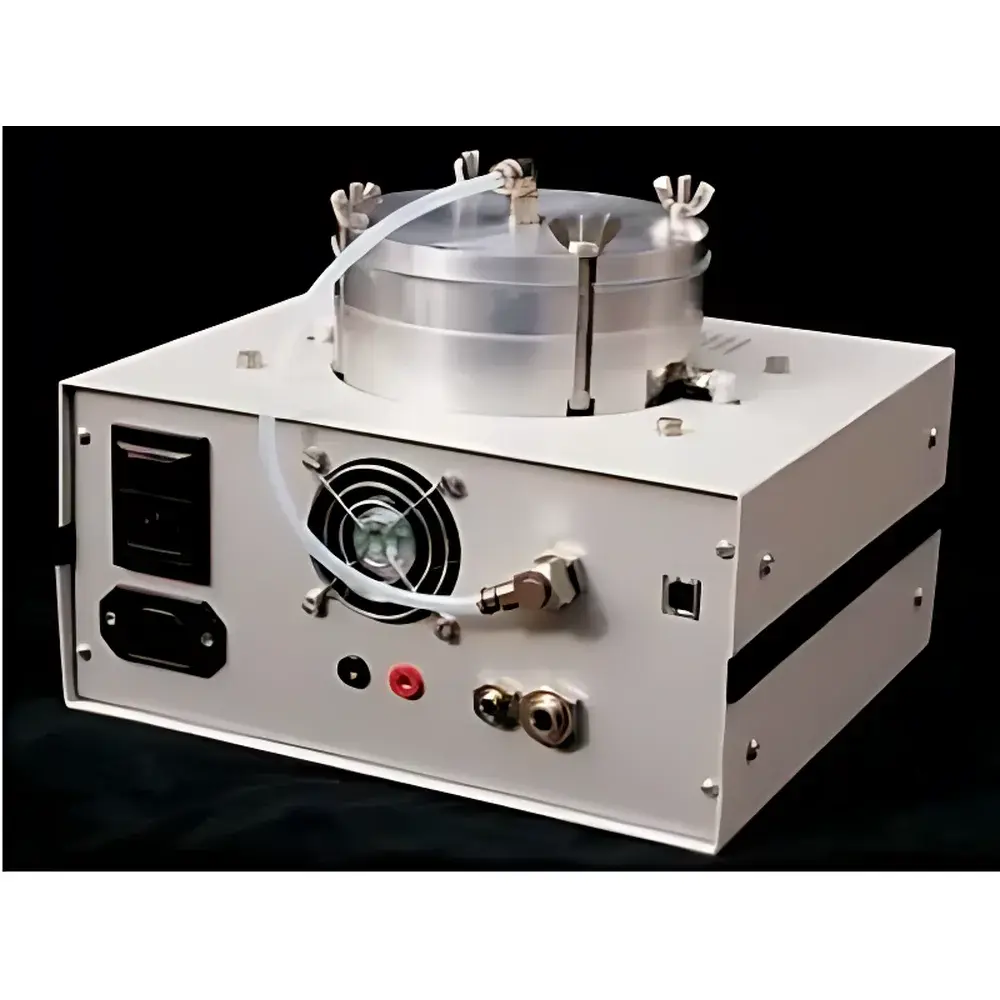
| Model | CN1 |
| Price Range | USD 7,000 – 14,000 (FOB Copenhagen) |
| Minimum Feature Size | 20 nm |
| Thermal Imprint Temperature | 200 °C (upgradable to 240 °C) |
| UV Wavelength | 365 nm |
| Pressure Range | 0.3–11 bar |
| Vacuum Level | down to 0.1 mbar |
| Substrate/Template Max Diameter | 100 mm (4-inch), upgradable to 200 mm (8-inch) |
| Control | Fully computer-programmed, GUI-driven operation |
| Brand | NILT |
|---|---|
| Origin | Imported |
| Manufacturer Type | Authorized Distributor |
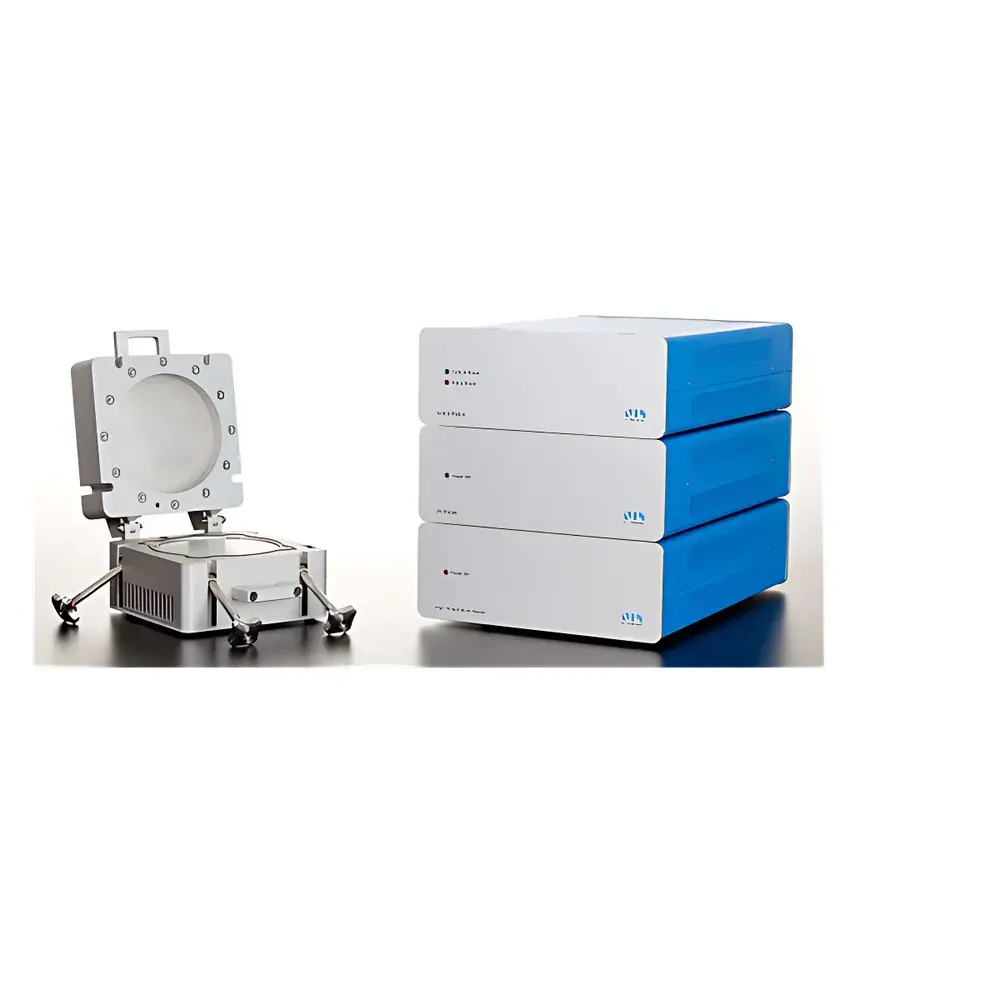
| Model | CNI |
| Price Range | USD 42,000–70,000 (FOB) |
| Minimum Feature Size | <20 nm |
| Imprint Area Compatibility | 2-inch to 4-inch wafers (customizable) |
| Heating/Cooling Rate | Rapid thermal cycling (<60 s ramp-up/down) |
| Vacuum Requirement | 0.4–0.8 bar (vacuum flow ≥1 mL/min) |
| Pneumatic Supply | Compressed air or N₂ at 6–10 bar |
| Electrical Input | 110–240 V AC, 50–60 Hz, ≥200 W |
| Brand | NILT |
|---|---|
| Origin | Denmark |
| Manufacturer Type | Authorized Distributor |
| Origin Category | Imported |
| Model | CNI V4.0 PV |
| Pricing | Upon Request |
| Imprint Area | Up to Ø210 mm (8″) |
| Chamber Height | 20 mm |
| Thermal NIL Max Temp | 200 °C (optional 250 °C module) |
| UV-NIL Wavelength | 365 nm (optional 405 nm module) |
| Vacuum Level | ≤0.1 mbar |
| Maximum Imprint Pressure | 11 bar |
| Control Interface | Laptop-based with dedicated software |
| Automation Level | Fully automated process execution (manual stamp/substrate loading) |
| Form Factor | Benchtop, modular, plug-and-play |