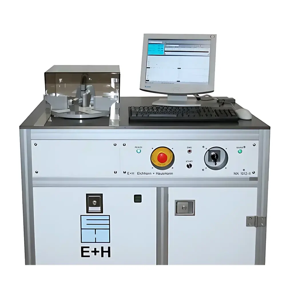
E+H Metrology MX 1012 High-Resolution Wafer Thickness and Total Thickness Variation (TTV) Measurement System
| Brand | E+H Metrology |
|---|---|
| Origin | Germany |
| Manufacturer Type | Authorized Distributor |
| Origin Category | Imported |
| Model | MX 1012 |
| Pricing | Upon Request |
| Wafer Diameter | 200 mm, 300 mm |
| Accuracy | ±0.1 µm |
| Resolution | 10 nm |
| Spatial Resolution | 1 mm |
| Max Scan Passes | 8 |
| Software | MX-NT |
Overview
The E+H Metrology MX 1012 is a non-contact, high-precision metrology system engineered for quantitative thickness and total thickness variation (TTV) characterization of silicon wafers in semiconductor front-end process environments. It operates on the principle of differential capacitive sensing—utilizing two opposing, temperature-stabilized capacitive transducers to measure absolute wafer thickness at discrete spatial points with sub-micrometer repeatability. Unlike optical interferometric or laser triangulation methods, capacitive measurement provides inherent immunity to surface reflectivity variations, oxide layer interference, and ambient light fluctuations—critical advantages when evaluating post-grind, post-polish, or bare-silicon wafers. The system is designed for integration into cleanroom-compatible automated material handling systems (AMHS), supporting SECS/GEM communication protocols and standard robotic end-effector interfaces. Its compact footprint and modular sensor head architecture enable deployment in both R&D laboratories and high-throughput production lines where real-time TTV feedback is essential for process window validation and yield optimization.
Key Features
- Dual-capacitive sensor architecture enabling simultaneous top- and bottom-surface displacement detection with nanometer-level resolution (10 nm)
- Four radial scan profiles at 45° angular increments per wafer, each comprising >200 discrete thickness measurements spaced at 1 mm intervals
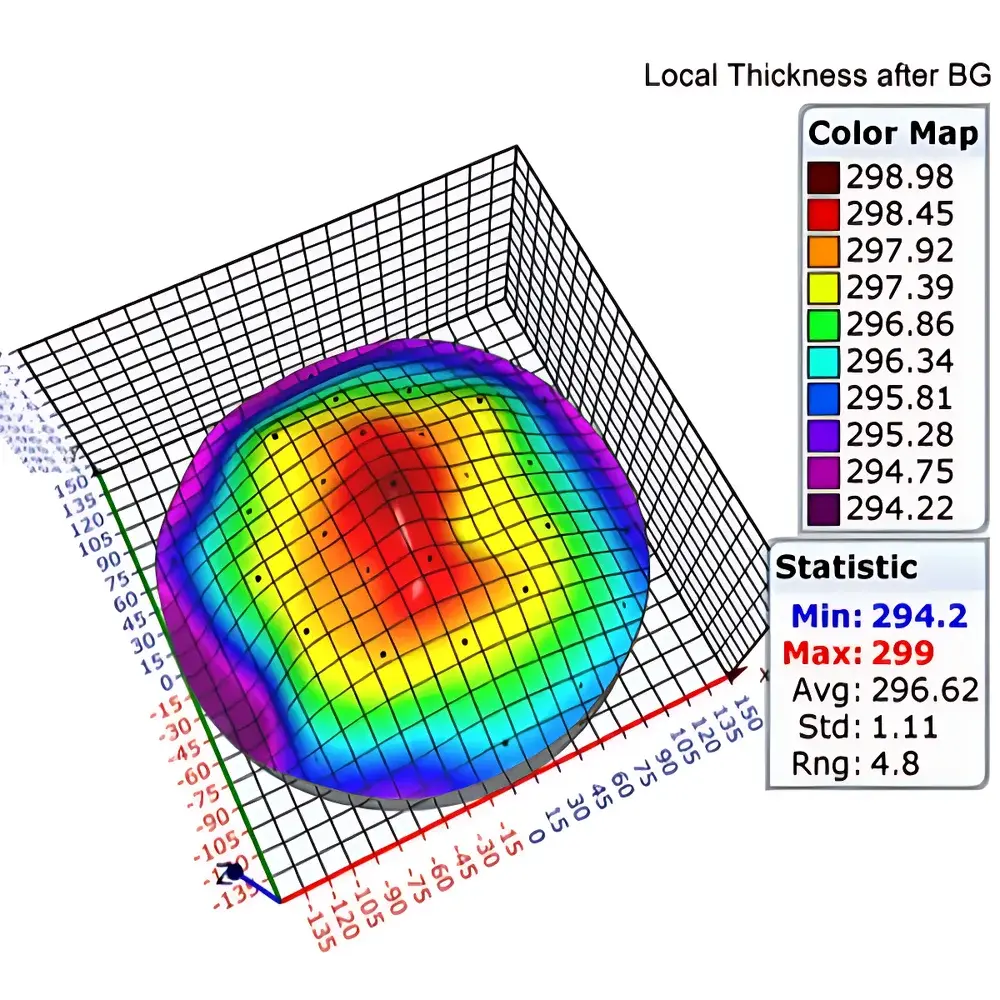
- Configurable up to eight full-diameter scans for enhanced spatial coverage—ideal for detecting edge roll-off, center-thickness deviation, and warp-induced asymmetry
- Integrated thermal drift compensation and air-bearing stabilized Z-axis motion ensure long-term measurement stability (<0.05 µm/8 h)
- Robust mechanical design compliant with SEMI S2/S8 safety standards and ISO 14644-1 Class 5 cleanroom requirements
- Real-time thickness mapping with color-coded TTV heatmaps and statistical summary (mean, std dev, min/max, 3σ spread)
Sample Compatibility & Compliance
The MX 1012 supports standard silicon wafers of 200 mm and 300 mm diameter, including those with native oxide, thermal oxide, nitride capping layers, and post-CMP surfaces. It accommodates wafer thicknesses ranging from 200 µm to 1,200 µm without hardware reconfiguration. The system meets ASTM F39–22 (Standard Test Method for Measuring Thickness of Silicon Wafers Using Capacitance Techniques) and aligns with SEMI MF-1530 specifications for TTV measurement uncertainty. All calibration procedures are traceable to PTB (Physikalisch-Technische Bundesanstalt) reference standards. Data acquisition and storage comply with FDA 21 CFR Part 11 requirements via audit-trail-enabled MX-NT software, supporting electronic signatures and role-based access control for GLP/GMP-regulated environments.
Software & Data Management
MX-NT is a Windows-based, deterministic real-time control and analysis platform developed exclusively for E+H Metrology wafer metrology systems. It provides synchronized motor control, sensor signal conditioning, and raw capacitance-to-thickness conversion using factory-calibrated polynomial coefficients. The software includes built-in statistical process control (SPC) modules compliant with ISO 22514–2, enabling real-time X-bar/R charting, capability indices (Cp/Cpk), and automated out-of-spec alerts. Measurement data is stored in HDF5 format with embedded metadata (timestamp, operator ID, recipe name, environmental conditions). Export options include CSV, XML, and SEMI E57-compliant binary formats for integration with MES (Manufacturing Execution Systems) and yield management platforms such as Applied Materials Yield Manager or PDF Solutions Exensio.
Applications
- Post-grinding and post-lapping process qualification—verifying thickness uniformity before CMP
- Rapid TTV screening during wafer reclaim and reuse evaluation
- Tool matching and cross-fab correlation studies across multiple grinding/polishing tools
- Development of thickness control recipes for advanced packaging substrates (e.g., TSV wafers, fan-out redistribution layers)
- Root cause analysis of wafer bow, warp, and stress-induced thickness gradients in epitaxial and SOI structures
- Supporting ITRS-defined metrology requirements for sub-10 nm node process control
FAQ
Does the MX 1012 require vacuum or nitrogen purging for operation?
No—capacitive sensing is insensitive to atmospheric composition; operation under standard cleanroom ambient conditions (22 ± 1 °C, 45 ± 5% RH) is sufficient.
Can MX-NT generate SPC reports compliant with ISO 9001 internal audits?
Yes—MX-NT includes configurable SPC templates, automated report generation, and full audit trail logging required for ISO 9001:2015 Clause 8.5.1 verification records.
Is the system compatible with FOUP or SMIF load ports?
Yes—the MX 1012 integrates with standard 300 mm FOUP handlers via SECS/GEM interface and supports manual loading for 200 mm wafers using a dedicated chuck fixture.
What maintenance intervals are recommended for long-term accuracy retention?
Annual recalibration against NIST-traceable step-height standards is recommended; daily zero-point verification using certified reference wafers is performed automatically during startup.


