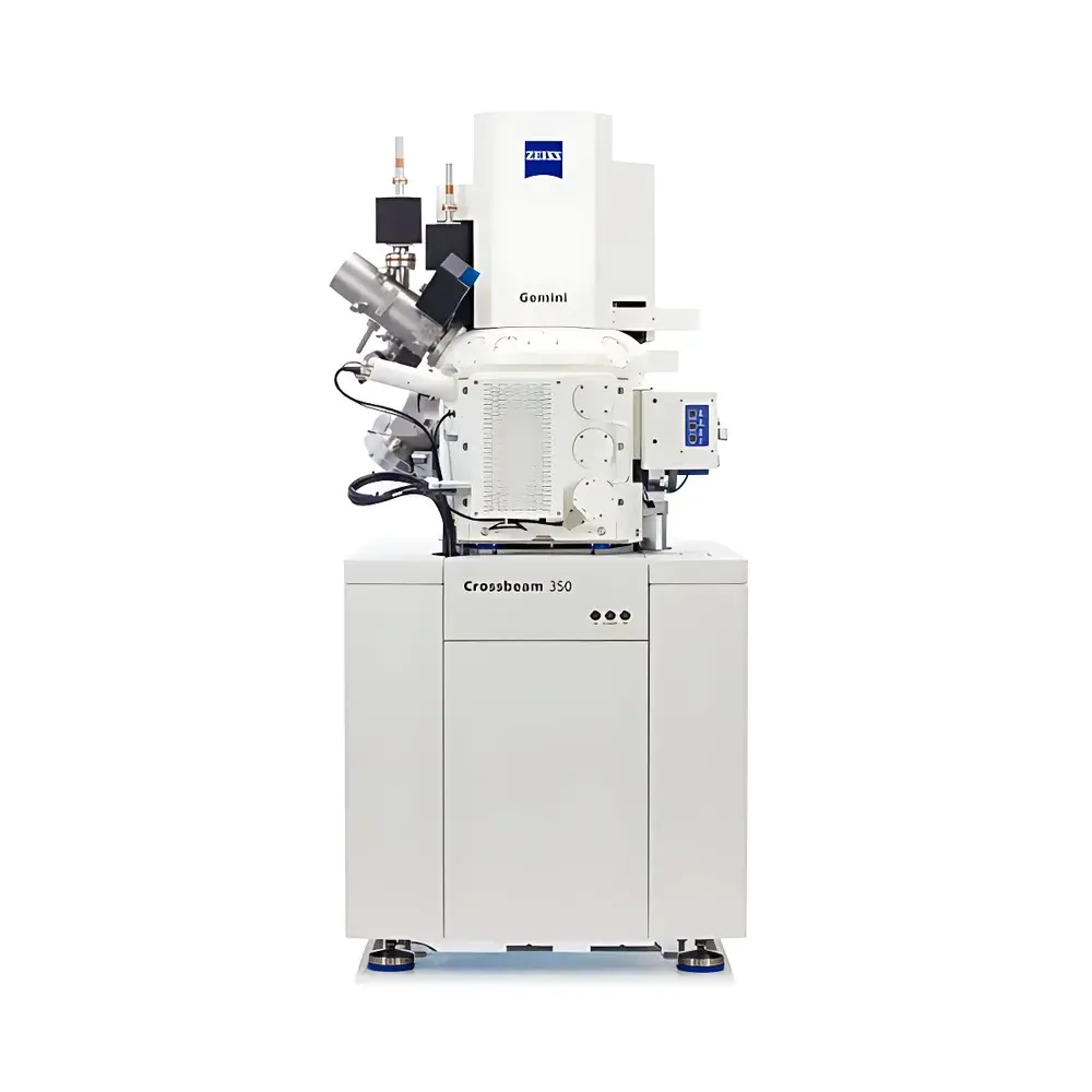
ZEISS Crossbeam 350 FIB-SEM DualBeam System
| Brand | ZEISS |
|---|---|
| Origin | Germany |
| Model | Crossbeam 350 |
| Configuration | Standard Chamber (18 ports) |
| Electron Optics | Gemini I with Tandem Decel |
| FIB Source | Liquid Metal Ga⁺ |
| Max FIB Current | 100 nA |
| SEM Resolution | ≤1.4 nm @ 1 kV (Tandem Decel) |
| Chamber Dimensions | Ø220 mm × H220 mm |
| Stage Travel | X/Y = 100 mm, Z = 40 mm |
| Detector Options | Inlens SE, Inlens EsB, VPSE, Inlens Duo |
| Software Platform | ZEISS Atlas 5 (3D Tomography & EDS Integration) |
| Compliance | Fully compatible with ASTM E1558, ISO/IEC 17025 workflows, GLP/GMP audit-ready data traceability (via Atlas 5 metadata logging) |
Overview
The ZEISS Crossbeam 350 is a high-precision dual-beam focused ion beam–scanning electron microscope (FIB-SEM) engineered for nanoscale 3D characterization, site-specific sample preparation, and correlative microanalysis. Integrating ZEISS’s Gemini I electron optical column—featuring Tandem Decel low-voltage deceleration technology—with a high-current liquid metal gallium (Ga⁺) focused ion beam column, the system delivers sub-2 nm surface-sensitive SEM imaging and rapid, high-fidelity ion milling in a single vacuum chamber. Unlike conventional sequential analysis platforms, the Crossbeam 350 enables true concurrent operation: real-time SEM monitoring during FIB milling, in situ cross-sectioning, TEM lamella lift-out, and automated 3D tomographic serial sectioning. Its architecture supports rigorous metrology-grade workflows across semiconductor failure analysis, advanced battery electrode studies, metallurgical phase mapping, and geological microstructure quantification.
Key Features
- Gemini I electron column with Tandem Decel: Achieves ≤1.4 nm resolution at 1 kV accelerating voltage, enabling high-contrast, low-damage imaging of beam-sensitive or non-conductive materials without conductive coating.
- High-current Ga⁺ FIB source: Delivers up to 100 nA ion current with stable, round beam profiles—critical for fast, high-aspect-ratio trenching (e.g., 100 × 30 × 25 µm³ in Si in <10 min) and reproducible TEM lamella thinning.
- Fastmill ion scanning strategy: A proprietary angle-optimized raster algorithm that increases material removal rates by up to 40% compared to conventional linear milling—validated on Si, Cu, and multilayer Ag-Ni-Cu structures.
- Inlens EsB (Energy-selective Backscattered) detector: Provides atomic-number (Z)-contrast imaging with <3 nm effective detection depth, enabling compositional mapping independent of topography and immune to charging artifacts.
- Modular chamber design: Standard 18-port configuration; optional extended chamber (22 ports) accommodates simultaneous integration of STEM detector, 4-quadrant BSE, local charge neutralizer, and pneumatic sample transfer stages.
- Atlas 5 software suite: Native 3D reconstruction engine with integrated energy-dispersive X-ray spectroscopy (EDS) voxel correlation—supports automated tilt-series acquisition, drift-corrected alignment, and quantitative elemental volume rendering aligned to structural tomograms.
Sample Compatibility & Compliance
The Crossbeam 350 accommodates diverse specimen geometries—from 8-inch wafers (with optional large pre-chamber) to irregular geological cores and biological cryo-sections. Variable pressure (VP) mode (optional on Crossbeam 340 variant) extends usability to partially outgassing or hydrated samples, though the 350 operates primarily under high vacuum (<1×10⁻⁵ mbar) for optimal FIB stability and EDS signal-to-noise. All hardware and software modules comply with ISO/IEC 17025 documentation requirements for accredited testing laboratories. Atlas 5 implements full 21 CFR Part 11–compliant audit trails—including user action logs, parameter versioning, and raw data fingerprinting—ensuring traceability for GLP and GMP-regulated R&D environments.
Software & Data Management
Atlas 5 serves as the unified control and analysis environment, unifying FIB navigation, SEM imaging, EDS acquisition, and 3D reconstruction into a single workflow interface. Its “AutoLamella” module executes fully scripted TEM sample preparation—including rough cut, polishing, lift-out, and final thinning—with positional repeatability better than ±100 nm. The “Tomography” module supports both slice-and-view and slice-and-scan modalities, with automatic stage repositioning, beam alignment correction, and adaptive dose control per slice. All acquired datasets—including SEM frames, EDS spectra, and reconstructed volumes—are stored in vendor-neutral HDF5 format with embedded metadata (accelerating voltage, dwell time, stage coordinates, detector gain), facilitating FAIR (Findable, Accessible, Interoperable, Reusable) data practices.
Applications
- Semiconductor device analysis: Cross-sectional imaging of FinFET gate stacks, interconnect void detection, and dopant profiling via EDS tomography.
- Materials science: Quantitative 3D grain boundary network reconstruction in X2CrNi18-10 stainless steel, including Cr-carbide precipitation mapping at heat-affected zones using STEM-EDS correlation.
- Energy storage: Nanoscale porosity and SEI layer thickness distribution analysis in Li-ion cathode particles after cycling.
- Geosciences: FIB-SEM serial sectioning of shale matrix to quantify organic matter distribution, pore throat connectivity, and mineral phase intergrowths.
- Life sciences: Targeted lamella preparation from frozen-hydrated tissue sections for cryo-TEM, guided by correlated fluorescence or CLEM markers.
FAQ
What is the maximum FIB current available on the Crossbeam 350?
The system is equipped with a Ga⁺ ion source capable of delivering up to 100 nA, optimized for high-speed milling while maintaining beam shape fidelity.
Does the Crossbeam 350 support EDS tomography?
Yes—Atlas 5 enables synchronized EDS spectrum acquisition during serial sectioning, with voxel-aligned elemental reconstruction and quantification against standardless or standards-based calibration.
Can non-conductive samples be imaged without sputter coating?
Absolutely. The Inlens EsB detector, combined with Tandem Decel at 1 kV, provides intrinsic charge compensation for ceramics, polymers, and biological specimens.
Is the system compatible with automated batch TEM lamella preparation?
Yes—AutoLamella in Atlas 5 supports unattended preparation of >35 lamellae per run, with positional accuracy verified via fiducial-based alignment and real-time SEM feedback.
What vacuum level is required for optimal FIB-SEM performance?
The FIB column requires ultra-high vacuum (<5×10⁻⁸ mbar), maintained by differential pumping; the main chamber operates at <1×10⁻⁵ mbar, ensuring long-term source stability and minimal ion beam scattering.


