NT-MDT Solver Next Atomic Force Microscope
| Brand | NT-MDT |
|---|---|
| Origin | Russia |
| Model | Solver Next |
| Instrument Type | Atomic Force Microscope |
| Z-direction Position Detection Noise | 0.02 nm (low-current mode) |
| Maximum Sample Dimensions | Ø ≤ 20 mm, Height ≤ 10 mm |
| XY Sample Stage Travel Range | 5 mm × 5 mm |
| Scan Range (Closed-loop) | 100 µm × 100 µm × 10 µm |
| Z-noise (RMS, 10–1000 Hz) | ≤ 0.04 nm (closed-loop), 0.02 nm (low-current mode) |
| XY Nonlinearity | ≤ 0.1% (closed-loop) |
| Video Microscope Resolution | 2 µm |
| Temperature Control Range | Room Temperature to 150 °C |
Overview
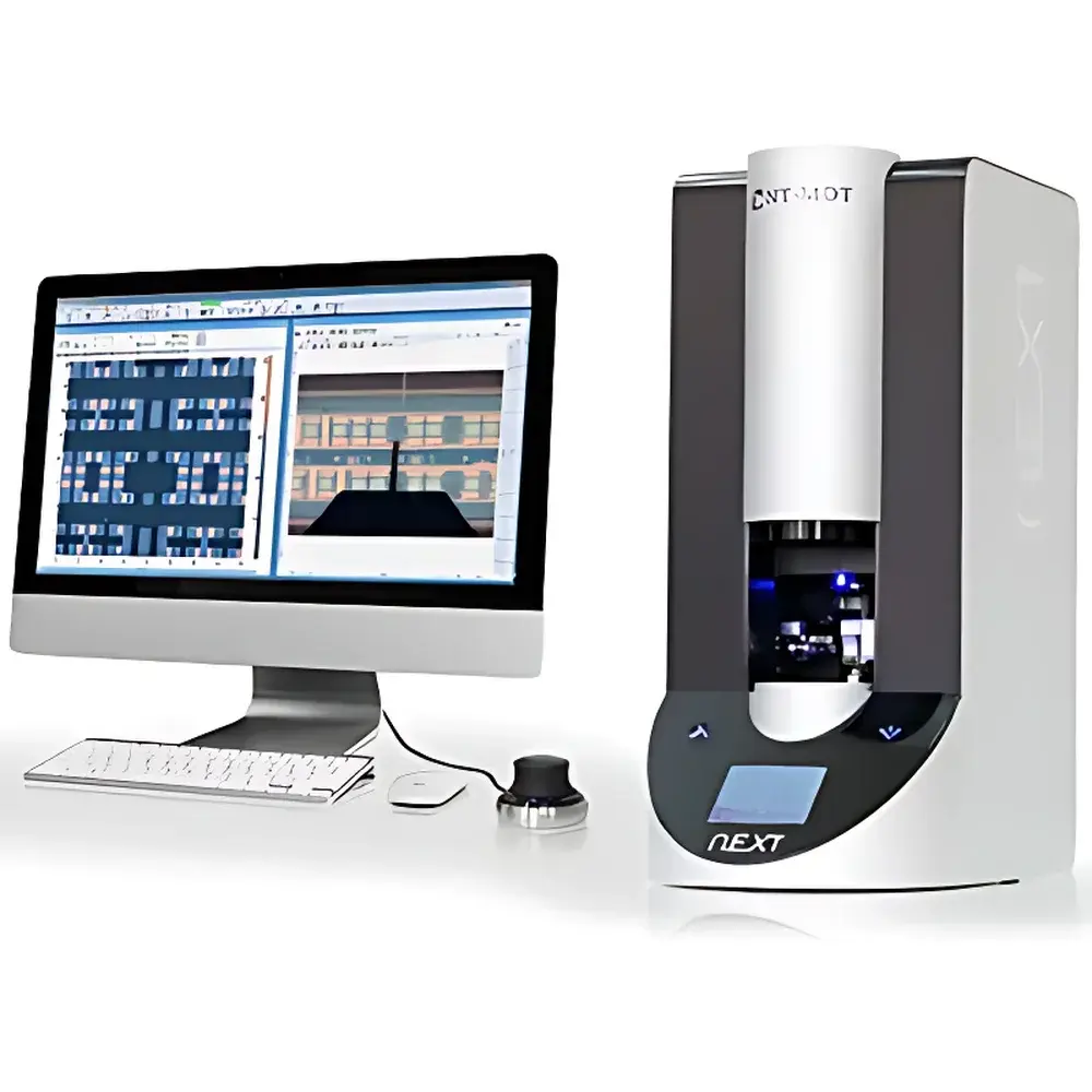
The NT-MDT Solver Next Atomic Force Microscope is a compact, high-performance scanning probe microscope engineered for precision nanoscale surface characterization in academic, industrial, and quality control laboratories. Based on the fundamental principles of atomic force microscopy—where interatomic forces between a sharp tip and sample surface are transduced via a microfabricated cantilever—the Solver Next delivers quantitative topographic, mechanical, electrical, and magnetic property mapping with sub-nanometer resolution. Its design integrates closed-loop piezoelectric positioning, real-time feedback compensation for hysteresis and creep, and a dual-mode scanning head capable of seamless switching between AFM and STM modalities without manual reconfiguration. Unlike conventional SPM systems requiring extensive operator training and iterative parameter tuning, the Solver Next implements an automated, workflow-driven architecture that reduces setup time from hours to minutes—enabling consistent, reproducible imaging across user skill levels while maintaining metrological integrity compliant with ISO/IEC 17025 traceability frameworks.
Key Features
- Integrated dual-mode scanning head with fully automated AFM/STM switching—no manual alignment or hardware exchange required.
- Closed-loop XYZ piezoscanner with 100 µm × 100 µm × 10 µm full-range travel and ≤0.1% XY nonlinearity, ensuring geometric fidelity in large-area scans.
- Ultra-low Z-direction detection noise: 0.02 nm RMS (10–1000 Hz bandwidth) in low-current mode—optimized for high-resolution force spectroscopy and nanomechanical mapping.
- Motorized optical path alignment system: automatic laser-cantilever-photodetector co-alignment ensures stable signal acquisition across environmental fluctuations.
- Software-controlled motorized sample stage with 5 mm × 5 mm travel and 0.3 µm minimum step resolution—enabling precise region-of-interest navigation and multi-location correlative analysis.
- High-resolution video microscope (2 µm resolution) with software-driven zoom, focus, field-of-view translation, and programmable stage synchronization.
- Ergonomic desktop footprint (W × D × H ≈ 600 × 550 × 450 mm) with motorized chamber door and integrated temperature control (RT to 150 °C) for in situ thermal studies.
Sample Compatibility & Compliance
The Solver Next accommodates standard disc-shaped samples up to 20 mm in diameter and 10 mm in height—compatible with common wafer, thin-film, polymer, biological, and electrochemical substrates. Its modular head design supports optional liquid-cell and nanoindentation modules, extending functionality to hydrated biomolecules, battery electrode interfaces, and viscoelastic thin films. All measurement modes—including contact, tapping, non-contact, lateral force, phase imaging, force modulation, adhesion mapping, MFM, EFM, Kelvin probe force microscopy (KPFM), spreading resistance, nanoindentation, and voltage/force-based nanolithography—are implemented under unified software control with parameter presets aligned to ASTM E2539 (Standard Guide for AFM Measurements) and ISO 25178-603 (Surface Texture: Nominal Characteristics). System firmware includes audit-trail logging and user-access-level management, supporting GLP/GMP-aligned workflows per FDA 21 CFR Part 11 requirements when deployed in regulated environments.
Software & Data Management
The proprietary Nova software platform provides a unified interface for instrument control, real-time data visualization, offline processing, and report generation. It features guided experiment wizards for novice users and scriptable macro environments (Python API) for advanced automation and integration into custom lab information management systems (LIMS). All raw sensor data—including photodiode quadrants, Z-piezo voltage, current, and timestamped metadata—are saved in open HDF5 format with embedded calibration parameters. Built-in tools support cross-sectional profiling, roughness analysis (Sa, Sq, Sz per ISO 25178-2), grain statistics, force-distance curve fitting (Hertz, Sneddon, DMT models), and spectral deconvolution. Software updates are delivered via secure HTTPS channels with version-controlled release notes and backward-compatible file handling.
Applications
The Solver Next serves as a versatile platform for nanoscale research and development across disciplines: semiconductor process monitoring (gate oxide uniformity, CMP defect analysis); nanomaterials characterization (graphene layer counting, CNT dispersion homogeneity); polymer science (phase separation kinetics, crystallinity mapping); life sciences (protein folding intermediates, cell membrane mechanics in buffer); energy materials (SEI layer morphology on Li-ion anodes, catalyst nanoparticle sintering); and failure analysis (corrosion initiation sites, interfacial delamination in multilayer coatings). Its closed-loop stability and low-noise performance make it particularly suitable for long-duration dynamic measurements such as creep-recovery tests, thermal expansion coefficient mapping, and electrochemical AFM (EC-AFM) under potentiostatic control.
FAQ
What scanning modes does the Solver Next support?
It supports STM, contact AFM, tapping mode, non-contact AFM, lateral force microscopy (LFM), phase imaging, force modulation, force spectroscopy, adhesion mapping, magnetic force microscopy (MFM), electrostatic force microscopy (EFM), Kelvin probe force microscopy (KPFM), spreading resistance imaging, nanoindentation, and voltage/force-assisted nanolithography.
Is the system compatible with liquid-phase measurements?
Yes—optional liquid-cell modules are available for in situ AFM in aqueous or organic solvents, enabling studies of biological macromolecules, electrochemical interfaces, and soft matter dynamics.
Can the instrument be integrated into automated laboratory workflows?
Yes—the Nova software provides a documented Python API for remote control, script-based batch acquisition, and integration with third-party platforms including MATLAB, LabVIEW, and enterprise LIMS.
Does the system meet regulatory compliance requirements for QC labs?
It supports audit-trail logging, electronic signatures, role-based access control, and data integrity safeguards aligned with FDA 21 CFR Part 11 and ISO/IEC 17025 for accredited testing laboratories.
What is the typical delivery lead time for configuration-specific setups?
Standard configurations ship within 8–12 weeks from order confirmation; lead times for custom modules (e.g., heated liquid cells or high-speed scanners) are quoted individually based on engineering validation cycles.


